Designing a Printed Circuit Board (PCB) layout involves a series of complex steps that require precision and planning.
A well-planned PCB layout is essential for both functionality and manufacturability. By understanding the steps involved, engineers can avoid common pitfalls and produce high-quality PCBs.
This article will guide you through the essential steps of PCB assembly and layout design, from defining requirements to assembly, offering practical advice and insights along the way.
1. Clearly Define Requirements

Before starting the design process, it’s essential to gather all electronic and mechanical requirements.
Key factors to consider include the size of the board, the number of layers, and the operating environment.
Engaging stakeholders early in the process helps confirm these requirements and sets a solid foundation for the design.
Clear requirements are required for effective schematic design, as they inform the necessary specifications and constraints for the project.
For instance, a PCB intended for use in harsh environments needs different considerations compared to one used in consumer electronics.
Additionally, understanding the thermal and mechanical stresses that the PCB will face is required.
This early-stage planning helps in deciding on the right materials and construction techniques to use.
By involving all relevant parties from the beginning, you make sure that the design meets everyone’s needs and reduces the likelihood of costly changes later in the process.
2. Create a Schematic Design
A schematic design is a visual representation of the electronic circuits within the PCB.
It serves as the blueprint for laying out components on the board. Using the right software tools can greatly facilitate this process.
Double-checking connections and component values is essential to prevent errors.
An accurate schematic is the backbone of a reliable PCB, guiding the placement and routing of components.
When creating a schematic design, you to keep the design simple and avoid unnecessary complexity.
This simplicity makes it easier to spot errors and streamline the design process.
Using tools like Altium Designer or Eagle can help in creating precise schematics and all connections are correct.
Remember, a schematic design is not just about placing components; it’s about creating a clear, logical representation of the circuit that makes the subsequent layout step more straightforward.
3. Layout the Components

Transitioning from a schematic to actual component placement is a much-needed step in electronics manufacturing.
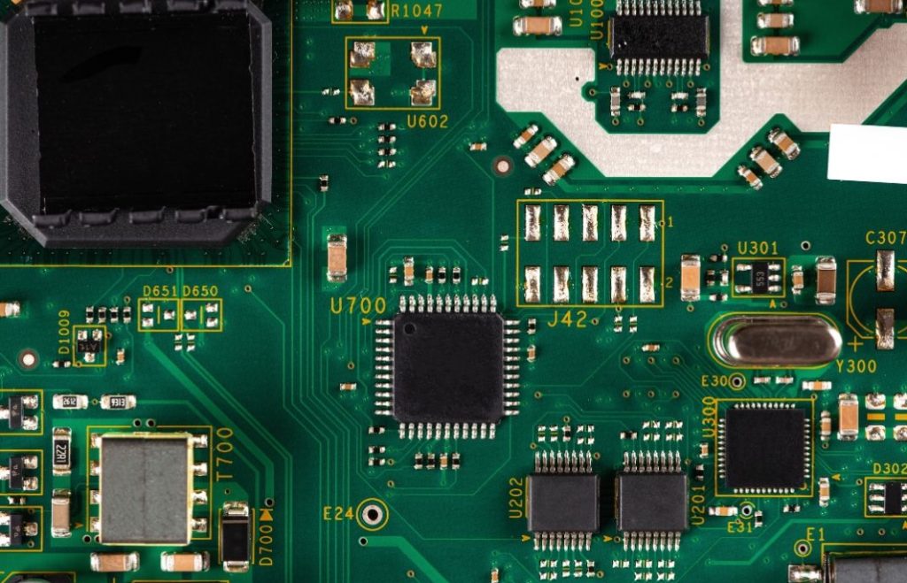
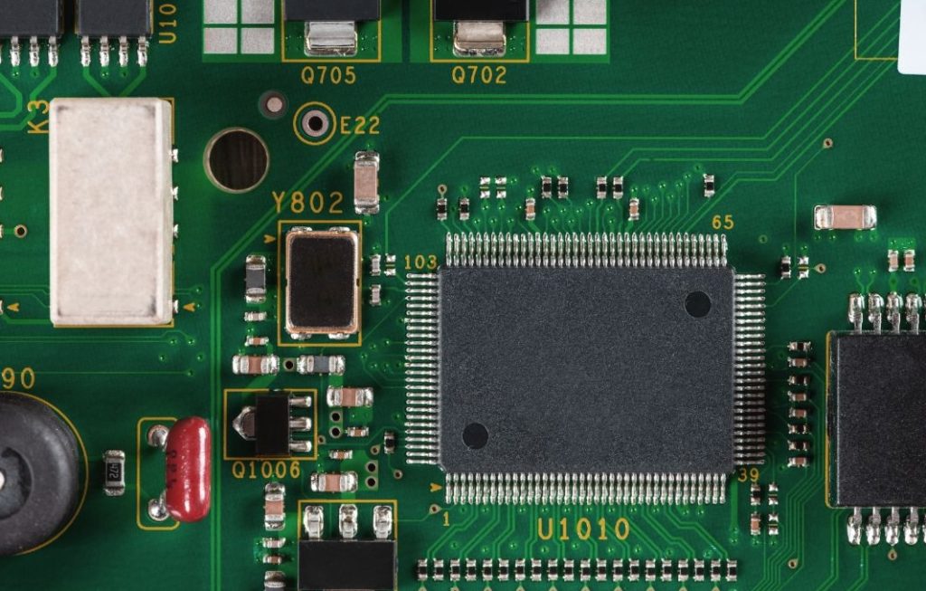
Deciding on the placement of components involves considering their relationships to each other, thermal management, and signal integrity.
Proper placement means that the board functions correctly and is easy to manufacture.
Guidelines on routing and connection strategies can help achieve a reliable and efficient design.
One key aspect of component layout is considering the power and ground planes.
These planes help in reducing noise and improving signal integrity. Placing decoupling capacitors close to the power pins of integrated circuits can also enhance performance.
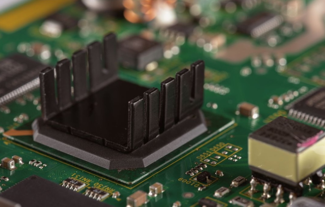
Additionally, considering the heat generated by components and planning for adequate cooling can prevent overheating issues.
4. Have your PCB Made
Once the layout is complete, the next step is converting the design into a physical board.
This involves choosing a PCB manufacturer and preparing the necessary files, such as Gerber files.
You need to review the manufacturer’s capabilities and quality assurance processes to match your design requirements.
Checking the design for manufacturability issues before final submission can save time and costs.
Selecting the right PCB manufacturer involves considering factors such as production capacity, technology, and track record.
Some manufacturers specialise in high-volume production, while others focus on prototyping or specialised technologies.
You need to make sure your chosen manufacturer can handle your specific requirements is essential.
Additionally, you might consider subcontracting PCB assembly to take advantage of specialised expertise and equipment.
5. Order Components
Selecting and ordering the electronic components for the PCB is another big step. Consider availability and cost when sourcing components, and verify that their specifications meet the design requirements.
Building relationships with reliable suppliers can help maintain quality and timely delivery.
Proper component selection is key to the overall performance and reliability of the PCB.
When ordering components, it’s beneficial to check for any long lead-time items that could delay your project.
Keeping an eye on market trends and potential shortages can help you make informed decisions about component sourcing.
Additionally, having backup suppliers can mitigate risks associated with supply chain disruptions.
Verifying component specifications against your design compatibility and performance, preventing issues during assembly and testing.
6. Assemble your PCB
The assembly process involves soldering components onto the PCB and performing thorough testing.
Depending on the complexity of the board, the assembly can be manual or automated.
Each method has its benefits and challenges.
Common assembly issues include solder bridges and misaligned components, which can be avoided with careful handling and inspection.
Testing is needed to make sure that the board operates as intended.
Manual assembly might be suitable for small production runs or prototypes, where flexibility and adjustments are necessary.
Automated assembly, on the other hand, is ideal for larger production runs, offering precision and efficiency.
Regardless of the method, thorough testing after assembly is essential.
This testing can include functional tests, visual inspections, and electrical tests to verify that the board meets all specifications.
In summary, designing a PCB layout involves several detailed steps: defining requirements, creating a schematic, laying out components, manufacturing the board, ordering components, and assembling the PCB.
Attention to detail and careful planning at each stage can significantly improve the quality and functionality of the final product.
For more information and professional support in PCB design and manufacturing, contact us at Altimex.


