

PCB delamination is a hidden reliability issue that can lead to costly product failures if not addressed early in the manufacturing process.
It occurs when the bonded layers within a printed circuit board begin to separate, weakening structural integrity and disrupting electrical performance.
For engineers and procurement teams, the challenge is not identifying the concept. The difficulty lies in understanding where delamination originates and how manufacturing decisions influence long-term reliability. Failures linked to delamination can be difficult to trace once a product is in use, which makes prevention during design, storage and assembly critical.
Our guide explains how PCB delamination develops, how to recognise early warning signs and how controlled manufacturing processes reduce risk.
PCB Delamination in Modern Electronics
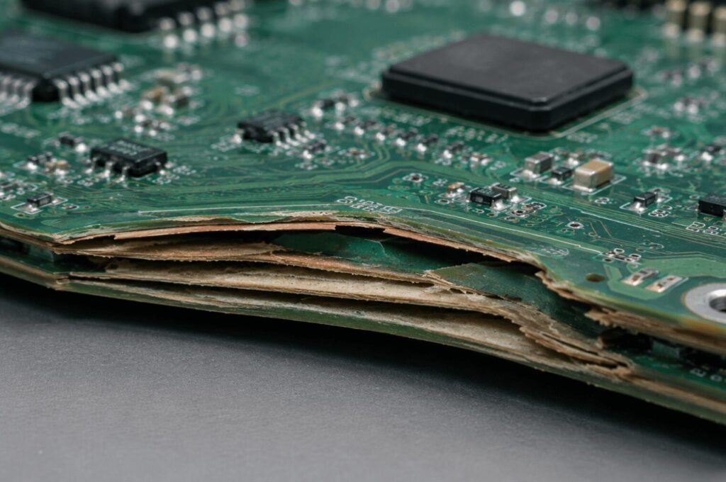
PCB delamination occurs when layers within a printed circuit board separate due to heat, moisture or mechanical stress, reducing reliability and potentially causing electrical failure.
In practical terms, this separation happens between the laminated layers that form a multilayer PCB. These layers are bonded under controlled pressure and temperature. When that bond weakens, the structure of the board begins to fail internally.
Typical characteristics include:
- Visible bubbling or blistering on the surface
- Localised lifting between layers
- Discolouration caused by heat exposure
- Subtle warping in affected areas
Multilayer PCBs are particularly vulnerable due to their complex structure. Each additional layer introduces another interface where bonding must remain stable under thermal and mechanical stress.
In modern electronics, where boards are more compact and operate at higher temperatures, the margin for error is reduced. A board used in industrial equipment, exposed to repeated heating and cooling cycles, can gradually develop internal stress. Over time, this can lead to separation even if the initial manufacturing process appeared acceptable.
For manufacturers, this reinforces the importance of tightly controlled production conditions rather than relying on material specifications alone.
Scale Your Production
From prototype to full-scale electronic assembly, our UK facility is equipped to handle your requirements.
Get a QuoteCommon Causes of PCB Delamination
Most PCB delamination issues originate from excessive thermal stress, moisture absorption or poor manufacturing process control.
The causes can be grouped into two categories: manufacturing-stage defects and field-use stress.
Manufacturing-related causes
- Incorrect lamination pressure or temperature
- Poor bonding between substrate layers
- Inconsistent material quality
- Excessive heat during soldering or rework
- Contamination during assembly
Operational and environmental causes
- Repeated thermal cycling during use
- Moisture ingress before or after assembly
- Mechanical stress from vibration or handling
- Long-term exposure to high operating temperatures
A key distinction is whether the issue is preventable during production. Many delamination failures originate from process inconsistency rather than unavoidable environmental conditions.
For example, a board exposed to uncontrolled soldering temperatures during assembly may leave production with weakened internal bonds. In contrast, a well-manufactured board subjected to extreme thermal cycling in the field may degrade gradually over time.
Understanding this difference helps businesses identify whether the root cause lies in design, manufacturing or application.
Heat Exposure During PCB Manufacturing
Incorrect thermal profiles during PCB assembly can weaken bonding materials and increase the likelihood of internal layer separation.
Heat is introduced at multiple stages of PCB production, particularly during soldering processes such as reflow. Each material within the board expands at a different rate when exposed to temperature changes. If this expansion is not managed carefully, stress builds between layers.
Key risk areas include:
- Reflow soldering profiles exceeding material tolerances
- Uneven heating across high-density boards
- Repeated thermal exposure during rework
- Poor calibration of assembly equipment
For example, a localised repair using excessive heat can damage a small section of the board. While the defect may not be immediately visible, the bond between layers may already be compromised.
High-density PCBs require tighter control due to concentrated heat zones. Without consistent monitoring, even small variations in temperature can lead to long-term reliability issues.
This is where controlled PCB assembly processes become critical. Manufacturers must define and maintain precise thermal profiles rather than relying on general guidelines.
Engineering-Led Solutions
Work with a team that understands modern electronics and end-to-end manufacturing.
Our ExpertiseMoisture Absorption and PCB Reliability
Moisture trapped within PCB materials can expand rapidly during heating processes, causing internal stress and layer separation.
PCB substrates and laminates can absorb moisture from the surrounding environment. When these materials are exposed to heat during soldering, the trapped moisture expands into vapour. This creates internal pressure, which can force layers apart.
This effect is sometimes referred to as “popcorning”, where internal expansion leads to visible or hidden damage.
Common causes of moisture-related delamination include:
- Storage in uncontrolled humidity conditions
- Extended exposure to open air before assembly
- Lack of moisture barrier packaging
- Failure to precondition moisture-sensitive boards
A typical scenario involves boards stored in a warehouse without humidity control. By the time they reach the assembly stage, moisture has already been absorbed. During reflow, the rapid temperature increase triggers expansion within the material.
Preventive measures include:
- Using sealed moisture barrier bags
- Controlling storage environments
- Limiting exposure time before assembly
- Applying pre-bake processes where required
Effective moisture control is a handling discipline, not just a material consideration. Without it, even high-quality boards can fail during assembly.
Warning Signs of PCB Delamination
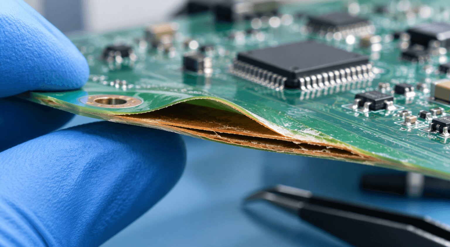
Visible warping, bubbling or discolouration are often early signs that PCB delamination may already be developing.
Early identification is critical, as many boards continue to function while internal separation progresses. Without inspection, these issues can pass through testing and only appear as intermittent faults in the field.
Common warning signs include:
- Surface blistering or bubbling, particularly after thermal exposure
- Localised swelling or raised areas on the board surface
- Discolouration linked to heat stress during assembly
- Warping or distortion affecting board flatness
- Fine cracking sounds during heating or handling
- Intermittent electrical instability during testing
In production environments, these signs are frequently detected during visual inspection or functional testing. For example, a slight surface blister following reflow may indicate trapped moisture expanding within the substrate.
Ignoring early indicators increases the likelihood of progressive failure. Consistent inspection procedures help isolate affected boards before they reach end use, reducing downstream reliability risks.
Ready to start your project?
Contact our technical team today to see how Altimex can streamline your electronics supply chain.
Contact UsPerformance Issues Linked to Delamination
Delamination can lead to intermittent electrical faults, reduced signal integrity and complete PCB failure over time.
As internal layers separate, electrical pathways are disrupted. This can affect both power delivery and signal transmission.
| Issue | Impact on Performance |
| Layer separation | Breaks internal connections |
| Signal degradation | Reduces communication accuracy |
| Thermal instability | Increases operating temperature variance |
| Open circuits | Causes complete failure in affected areas |
| Short circuits | Creates unpredictable system behaviour |
Multilayer boards are particularly sensitive due to their reliance on stable internal connections. Further insight into layer interaction is covered in this guide to understanding PCB layers.
In high-reliability environments such as industrial systems, even minor degradation can lead to significant operational disruption. This highlights the commercial impact of delamination beyond technical performance.
Manufacturing Processes That Reduce Delamination Risks
Consistent process control during PCB manufacturing significantly reduces the likelihood of delamination defects.
Prevention is achieved through disciplined production methods rather than isolated quality checks.
Key process controls include:
- Controlled thermal profiling
Ensuring all heating stages remain within defined material limits. - Material selection and traceability
Using consistent, verified substrates and laminates. - Lamination quality control
Maintaining correct pressure and temperature during layer bonding. - Moisture management procedures
Controlling storage and handling before assembly. - Inspection and testing protocols
Identifying defects at early production stages. - Process consistency across batches
Reducing variation between production runs.
A controlled environment produces predictable outcomes. In contrast, inconsistent processes introduce variability, which increases the likelihood of hidden defects.
For businesses, this reinforces the importance of selecting manufacturers who can demonstrate process discipline rather than relying on basic capability.
PCB Storage and Handling Best Practices
Improper storage and handling can undermine PCB reliability before assembly even begins.
Even when boards leave manufacturing in good condition, environmental exposure can introduce hidden risks. Moisture absorption, contamination and mechanical stress can all weaken the structure before the assembly process starts.
Best practices include:
- Store boards in humidity-controlled environments with monitored conditions
- Use sealed moisture barrier bags to limit environmental exposure
- Track floor life for moisture-sensitive materials before assembly
- Minimise handling to reduce contamination from oils or debris
- Use desiccants and humidity indicators within packaging
- Avoid stacking or flexing boards during storage and transport
A typical issue arises when boards are left unsealed in a warehouse for extended periods. Moisture gradually enters the material, yet the impact only becomes visible during soldering when heat triggers expansion.
Storage and handling should be treated as part of the overall quality process. Without control at this stage, earlier manufacturing standards can be compromised before assembly begins.
Thermal Management in PCB Design
Effective thermal management in PCB design helps reduce stress that can contribute to long-term delamination risks.
Design decisions directly influence how heat is distributed and dissipated across the board. Uneven heat concentration creates expansion differences between materials, which increases internal stress over time and weakens layer bonding.
Key considerations include:
- Balanced copper distribution to prevent uneven thermal expansion
- Strategic component placement to avoid concentrated heat zones
- Use of thermal vias to transfer heat away from critical areas
- Selection of materials suited to expected operating temperatures
- Designing for consistent heat flow across the entire board
Dense PCB layouts are a common risk factor. High-power components placed close together can create localised hot spots, placing continuous stress on the surrounding substrate.
Addressing thermal behaviour at the design stage reduces the burden on manufacturing controls. It also improves long-term reliability by limiting the conditions that lead to gradual layer separation.
Choosing a Reliable PCB Manufacturing Partner
A reliable PCB manufacturing partner should demonstrate strong process control, material quality standards and consistent quality assurance procedures.
For procurement teams, supplier evaluation is a critical step in reducing delamination risk.
Key questions to ask include:
- How are thermal profiles defined and monitored?
- What moisture control procedures are in place?
- How is material consistency verified across batches?
- What inspection methods are used to detect early defects?
- How are process variations controlled and documented?
- What experience exists with complex multilayer boards?
A manufacturer’s ability to answer these questions clearly is a strong indicator of reliability. Transparency and process discipline are more valuable than broad claims about quality.
If you are reviewing PCB reliability issues or evaluating manufacturing partners, Altimex can support discussions around suitable assembly processes and quality control approaches. You can contact us to explore your requirements.