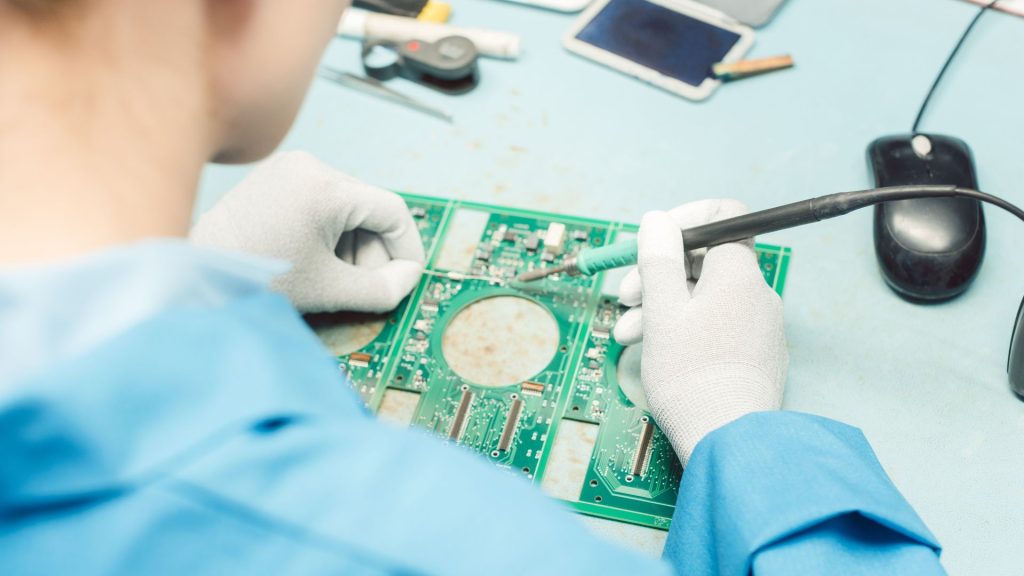
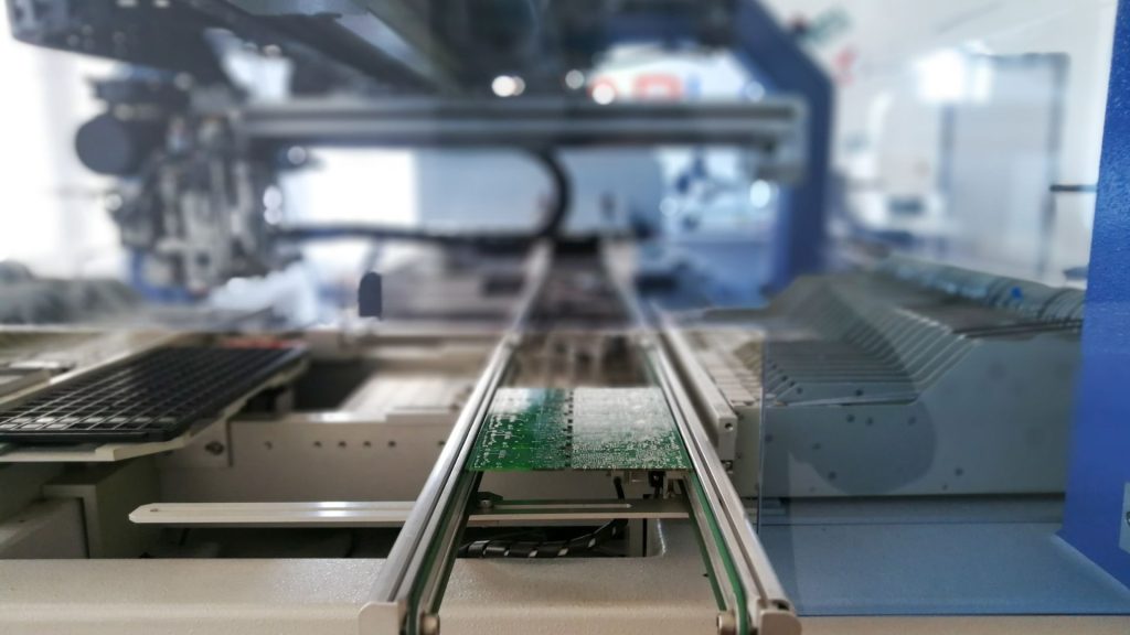
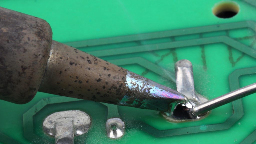
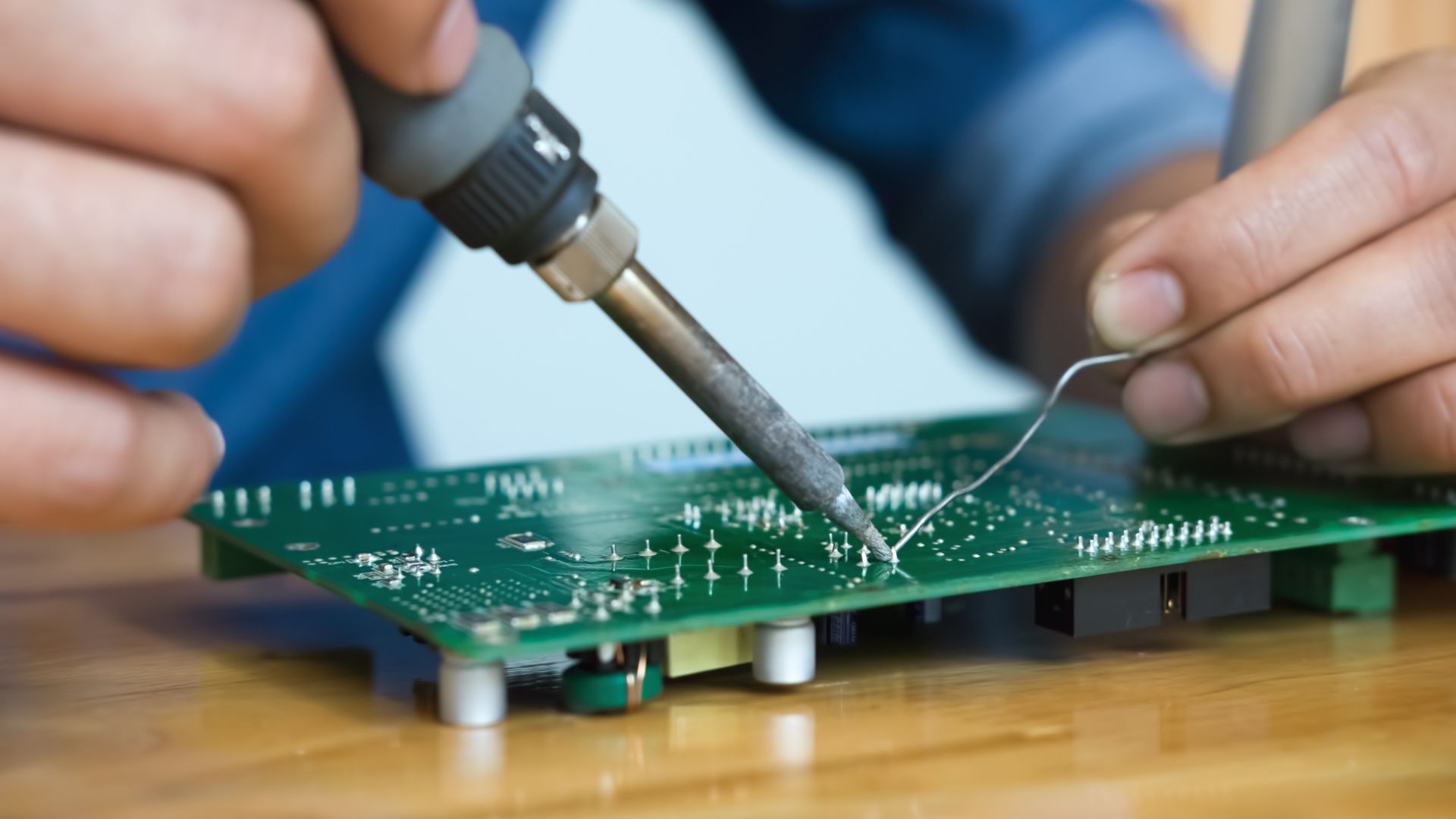
Printed Circuit Boards (PCBs) are essential components in modern electronics, providing the foundation for connecting various electronic parts. Found in devices ranging from smartphones to industrial machines, they play a major role in the functioning of countless technologies. Understanding how a PCB is made reveals the detailed and precise nature of electronics manufacturing.
The process of PCB manufacturing has advanced significantly over the years, moving from simple manual designs to complex computer-aided methods. These advancements have allowed for the creation of highly reliable and compact electronic circuits. Creating a PCB involves several detailed steps, each contributing to the board’s overall performance and quality.
So, how is a PCB board made? This article explores the step-by-step process of the creation process, from the initial design phase to the final testing stage. Whether you are an engineer, an electronics enthusiast, or simply curious about PCB production, this guide provides a thorough overview. By understanding each phase, you can appreciate the work that goes into making sure each version meets high standards of quality and functionality.
1. Designing the PCB

The first step is designing the board. This process begins with defining the requirements and initial concept. Engineers and designers use specialised software to create detailed schematics that map out the electrical pathways and components.
Tools such as Altium Designer, Eagle, and KiCad are commonly used in the design. These tools allow designers to create and modify schematics, ensuring all components are correctly placed and connected. The schematics serve as a blueprint, detailing how the electrical connections will be made.
During the designing PCB phase, it’s advised to consider both electrical and physical constraints, including factors such as signal integrity, thermal management, and component placement. Designers must think about the physical size and shape of the printed circuit board to fit within the intended device. Advanced tools and careful planning help achieve a functional and manufacturable layout.
2. Creating the PCB Layout
Once the schematic design is complete, the next step involves creating the physical layout of the board. This involves translating the schematic into a physical representation that can be produced. The layout includes placing components and routing the electrical connections or traces that link them.
The layout process starts with component placement, where designers strategically position each part on the board. This placement affects the board’s performance, manufacturability, and overall size. Following placement, the next step is routing the traces that connect the components, allowing electrical signals to travel efficiently across the board.
Design rules and checks are a major part of creating the layout. These rules ensure the board can be manufactured without issues and perform reliably in its intended application. Software tools like Altium Designer, Eagle, and KiCad are also used here to automate and validate these design rules.
For those needing assistance with PCB assembly, Altimex provides comprehensive services that support the entire process, achieving high-quality results. Using specialised software and adhering to strict design rules helps produce a reliable and functional layout that meets the required specifications.
3. Printing the PCB Design

The next phase in the process is printing the design onto the board material. This step involves transferring the layout from the digital design software onto the physical board. There are several methods used for this process, including inkjet printing, laser printing, and photolithography.
Inkjet Printing is a popular method due to its precision and ability to handle complex designs. It involves using a special inkjet printer to deposit conductive ink onto the board material.
Laser Printing uses a laser to etch the design onto the board, providing high accuracy and detail.
Photolithography is a more traditional method that involves coating the board with a photosensitive material and then exposing it to light through a mask of the design, creating a detailed pattern on the board.
Before printing, the board substrate must be prepared to allow proper adhesion of the design. This preparation includes cleaning the board to remove any contaminants that might interfere with the printing process. The accuracy of this step is crucial to avoid defects and ensure the board functions as intended.
Printing the design is a meticulous process that requires precision and attention to detail. It sets the stage for the subsequent steps in electronics manufacturing, ensuring that the final product meets the required specifications.
4. Etching the PCB
The etching process is a fundamental step in PCB manufacturing. This stage involves removing excess copper from the board to create the desired circuit patterns. The goal is to leave behind only the copper traces that form the electrical connections designed in the previous steps.
There are various etching techniques used in PCB manufacturing, with chemical etching being the most common. This method involves coating the board with a resist material that protects the desired copper areas. The board is then immersed in an etching solution, such as ferric chloride, which dissolves the exposed copper.
Another technique is laser etching, which uses a laser to precisely remove unwanted copper. This method offers higher accuracy and is particularly useful for intricate designs. However, it can be more costly compared to chemical etching.
Materials used for etching must be chosen carefully to match the board substrate and achieve the required precision. The entire process must be carefully controlled to avoid over-etching, which can damage the copper traces, or under-etching, which can leave excess copper on the board.
PCB etching shapes the electrical pathways on the board, directly affecting its performance. Proper etching techniques and materials are essential to produce a high-quality PCB that meets the design specifications.
5. Drilling Holes
The drilling process is an essential step in manufacturing, creating the necessary holes for component leads and vias. These holes allow electrical connections between different layers of the printed circuit board and facilitate the mounting of components.
Mechanical drilling is the most common method used, involving high-speed drills that can precisely create holes as small as 0.1mm in diameter. The accuracy of this process is crucial to achieve proper alignment and fit for the components. Laser drilling is another method used for creating even smaller holes with high precision, although it is generally more expensive.
The drilling process must be carefully controlled to avoid issues such as misalignment or damage to the board. Drills must be sharp and well-maintained to produce clean and accurate holes. Additionally, the board must be securely fixed during drilling to prevent movement that could affect the hole placement.
Vias are a specific type of hole that allows electrical connections between different layers of a multi-layer PCB. These are especially important in complex boards where space is limited, and efficient layer-to-layer connections are required.
Drilling is a process that requires precision and attention to detail, as it directly impacts the board’s functionality and the reliability of the electrical connections.
6. Plating and Coating
After drilling, the next step in the manufacturing process is plating and coating. This process involves applying a layer of metal, typically copper, to the drilled holes and the surface of the board. Plating creates electrical connections through the holes, linking different layers of the PCB.
The plating process begins with cleaning the board to remove any contaminants that might affect the adhesion of the metal layer. The board is then submerged in a chemical bath where an electric current is applied to deposit the copper evenly. This process, known as electroplating, creates a conductive path through the holes and across the surface of the board.
In addition to copper, other materials such as gold can be used for plating to improve conductivity and protect against corrosion. The choice of plating material depends on the specific requirements of the PCB.
Following plating, a protective coating is applied to the PCB. The most common type of coating is the solder mask, which covers the board’s surface except for the areas where components will be soldered. The solder mask prevents short circuits and protects the copper traces from environmental damage.
Other types of coatings, such as conformal coating, can also be used to provide additional protection, especially in harsh environments. These coatings contribute to the longevity and reliability of the printed circuit board by shielding it from moisture, dust, and chemicals.
7. Solder Mask Application

The solder mask application is an essential step in PCB manufacturing. The solder mask is a protective layer applied to the PCB’s surface, except for the areas where components will be soldered. This layer prevents short circuits, oxidation, and environmental damage, improving the overall durability of the PCB.
The process begins with cleaning the board to make sure the surface is free from dust and contaminants. A liquid photo-imageable solder mask is then applied to the PCB. The board is exposed to ultraviolet (UV) light through a stencil of the design, hardening the solder mask in the exposed areas while leaving the unexposed areas soft.
After exposure, the board is developed by washing away the soft, unexposed solder mask, revealing the areas where soldering will occur. The board is then baked in an oven to cure and harden the solder mask permanently.
There are different types of solder masks available, such as epoxy liquid, liquid photoimageable (LPI), and dry film solder masks. Each type has its specific applications and benefits, depending on the requirements of the PCB.
Quality control is needed during solder mask application to avoid defects such as bubbles, uneven coverage, or misalignment. Proper application helps the solder mask provide effective protection and contribute to the PCB’s reliability.
8. Silkscreen Printing
Silkscreen printing is a significant step in the manufacturing process. This stage involves printing useful information on the board, such as component labels, logos, and reference indicators. This information helps with assembly and troubleshooting by clearly identifying components and their placements.
The process begins with preparing the silkscreen, which is a stencil-like template that defines the areas to be printed. The board is cleaned to provide a smooth surface for the ink. Using the silkscreen, ink is applied to the board in the required areas, typically using a screen printer.
There are different techniques for silkscreen printing, including manual and automatic methods. Automatic silkscreen printing offers higher precision and consistency, making it suitable for large-scale production. The choice of ink is also crucial, as it must be durable and resistant to the operating conditions the board will face.
After printing, the board is usually baked to cure the ink, allowing it to firmly stick to the surface. The quality of silkscreen printing is essential to avoid issues like smudging, misalignment, or fading, which can hinder the readability of the printed information.
Silkscreen printing improves the usability of the board by providing clear and accurate labeling, aiding both in assembly and in future maintenance or repairs.
9. PCB Testing and Inspection
Testing and inspection are essential stages in production, confirming the board’s functionality and reliability before it is used in any electronic device. Various testing methods are employed to detect potential defects and verify the board’s performance.
Automated Optical Inspection (AOI) is one of the primary methods used. AOI involves using cameras to capture images of the board and compare them to the design specifications. This method helps identify issues such as missing components, incorrect placements, and soldering defects.
Another common method is X-ray inspection, which allows for the examination of internal layers and hidden solder joints that are not visible to the naked eye. X-ray inspection is particularly useful for detecting voids, cracks, and misalignments in multi-layer PCBs.
Functional testing involves evaluating the PCB’s performance under actual operating conditions. This test confirms that the board functions as intended when integrated into the final product. It includes checking electrical characteristics such as voltage, current, and signal integrity.
Any issues detected during testing are addressed and rectified to meet the required standards. Testing and inspection are crucial for maintaining the quality and functionality of the PCB, ultimately leading to reliable and high-performing electronic devices.
Understanding the detailed process of PCB manufacturing highlights the complexity and precision required at each step. From designing and creating the layout to printing, etching, drilling, plating, and thorough testing, each phase is critical to ensure the final product meets high standards of quality and functionality. Whether you are an engineer, an electronics enthusiast, or simply curious about PCB production, this comprehensive guide provides valuable insights into the meticulous work involved in bringing electronic circuits to life.
For more information on PCBs or to discuss your specific requirements, contact us at Altimex today.


