

Internet of Things (IoT) products depend on far more than connectivity and software functionality. Behind every connected device sits a printed circuit board (PCB) that must support reliable operation, efficient power consumption, wireless communication and long-term durability.
As IoT hardware becomes smaller and more capable, PCB manufacturing plays a bigger role in determining whether a product performs consistently in real-world conditions. Design decisions, material choices, assembly processes and quality controls all influence how a connected device behaves throughout its lifecycle.
IoT devices must balance compact design, connectivity, reliability and scalability within demanding manufacturing constraints. For organisations developing connected hardware, understanding how PCB manufacturing affects performance can reduce development risk, improve reliability and support a smoother transition from prototype to production.
Close collaboration between engineering teams and manufacturing specialists also helps ensure designs remain practical, scalable and commercially viable.
PCB Design Requirements for IoT Devices
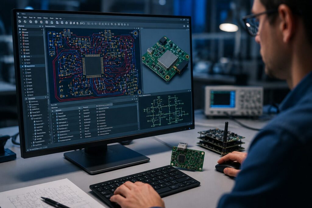
IoT devices require PCB designs that balance compact layouts, connectivity, power efficiency and long-term reliability.
Unlike traditional electronic products, connected devices typically combine sensors, wireless communication modules, power management circuits and processing components within a limited footprint. Each element must coexist without compromising electrical performance or manufacturability.
A compact environmental monitoring device provides a useful example. The PCB may need to accommodate temperature sensors, humidity sensors, a wireless communication module, battery management circuitry and a microcontroller within a housing designed for discreet installation. Every component placement decision affects routing complexity, thermal behaviour and assembly requirements.
Manufacturability should remain a priority from the earliest design stages. A PCB layout may function perfectly in a prototype while introducing avoidable assembly challenges during production. Design choices involving component spacing, pad geometry, routing density and test-point access can all influence manufacturing efficiency and long-term consistency.
Working closely with a specialist in PCB assembly during development helps engineering teams identify production constraints early. This may include component spacing issues, solderability concerns, assembly access limitations or insufficient test coverage that could become costly later.
Successful IoT PCB design requires balancing electrical performance with practical manufacturing realities. The strongest designs achieve both.
Scale Your Production
From prototype to full-scale electronic assembly, our UK facility is equipped to handle your requirements.
Get a QuoteMiniaturised PCB Designs for Compact Technology
Miniaturised IoT devices require densely packed PCB layouts that increase manufacturing and assembly complexity.
Many connected products are designed for compact enclosures. Wearables, smart sensors and portable monitoring equipment all place significant pressure on available board space.
As layouts become more condensed, engineers often rely on fine-pitch components and multilayer PCB architectures to achieve required functionality. These approaches enable compact designs but also increase manufacturing precision requirements.
Component placement tolerances become tighter. Soldering processes demand greater accuracy. Inspection procedures become more critical. Minor manufacturing deviations can have a much greater impact when circuits are densely populated.
Wearable technology illustrates this well. A fitness tracker may contain wireless communication hardware, battery management systems, sensors and processing components inside a very small enclosure. Achieving reliable assembly under these conditions requires close coordination between design and manufacturing teams.
Thermal density also becomes a major concern. As more functionality is concentrated into smaller areas, heat generation becomes localised, increasing the importance of layout planning and thermal management.
Miniaturisation is not simply a design challenge. It is equally a manufacturing challenge requiring precision, consistency and careful planning.
Reliable PCB Manufacturing for Connected Devices
Reliable PCB manufacturing is critical for IoT devices because connected products often operate continuously in demanding environments.
Many IoT systems are deployed in locations where maintenance access is limited. Industrial monitoring equipment, environmental sensors and infrastructure management systems may be expected to function for long periods without interruption.
Manufacturing quality directly affects operational reliability. Variations in solder joints, assembly consistency or substrate quality can introduce failures that may not appear until devices are deployed in the field.
Industrial IoT monitoring systems provide a useful example. A sensor installed within a manufacturing facility may operate continuously while exposed to vibration, temperature variation and airborne contaminants. Reliability depends not only on circuit design but on manufacturing consistency throughout the assembly process.
Quality assurance procedures help minimise these risks. Inspection, process control and validation testing help ensure production units perform consistently across manufacturing batches.
Reliability should never be treated as a final-stage consideration. It begins during design and continues through fabrication, assembly and testing.
For organisations investing in connected hardware, manufacturing consistency remains one of the strongest contributors to long-term product performance.
Engineering-Led Solutions
Work with a team that understands modern electronics and end-to-end manufacturing.
Our ExpertiseWireless Connectivity Within IoT Electronics
Wireless communication performance depends heavily on PCB layout, antenna placement and signal integrity.
Connectivity defines IoT hardware. Whether a product uses Wi-Fi, Bluetooth, LoRaWAN or another wireless technology, PCB design directly affects communication quality.
Antenna positioning requires careful consideration. Nearby components, metallic structures and routing decisions can affect signal transmission and reception. Poor placement may reduce range, create interference or introduce inconsistent performance between units.
Signal routing is equally important. High frequency communication paths require careful layout planning to preserve signal integrity. Trace lengths, grounding structures and layer transitions can all affect wireless performance.
Consider a Bluetooth enabled monitoring device. If antenna placement is compromised by surrounding circuitry or enclosure constraints, communication reliability may suffer even when premium components are used.
Shielding strategies can also help control electromagnetic interference. Multilayer PCB designs often support stronger grounding arrangements and improved signal separation, reducing interference between subsystems.
From a manufacturing perspective, consistency in antenna placement and assembly quality helps ensure predictable wireless performance across production runs; effective connectivity begins at PCB level.
Thermal Management in IoT Device Design
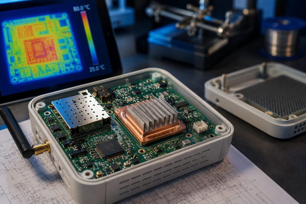
Thermal management becomes increasingly important as IoT devices become smaller and more functionally dense.
Every electronic component generates heat during operation. In compact IoT devices, limited enclosure space can make heat dissipation difficult.
Excessive temperatures can reduce performance, shorten component lifespan and increase reliability risks. Thermal management therefore forms an important part of both PCB design and manufacturing planning.
Component placement plays a major role. Heat generating components should be positioned to avoid concentrated hotspots. Thermal vias can help transfer heat between PCB layers and improve thermal distribution.
Battery powered IoT devices present a common challenge. Processing components, wireless modules and power management circuits may all generate heat inside restricted enclosures. Without proper thermal planning, operating temperatures can rise significantly during normal use.
Material selection also affects thermal performance. Different substrate materials offer varying thermal characteristics that influence heat transfer and long-term stability.
Successful thermal management combines thoughtful layout, suitable materials and consistent manufacturing practices.
Ready to start your project?
Contact our technical team today to see how Altimex can streamline your electronics supply chain.
Contact UsMulti Layer PCBs and Advanced IoT Functionality
Multilayer PCBs support advanced IoT functionality by enabling compact layouts, improved routing and better signal management.
As connected products become more sophisticated, single-layer and double-layer PCB designs often struggle to accommodate growing functionality within limited space.
Multilayer boards provide additional routing capacity, allowing engineers to separate power, ground and signal layers more effectively. This supports cleaner layouts and more complex circuit architectures.
Smart industrial control systems demonstrate the benefit clearly. A single device may contain multiple communication interfaces, sensors, processors and power management functions. Integrating all of these into a compact enclosure becomes significantly easier with multilayer construction.
Signal separation also improves performance. Dedicated layers help reduce EMI and support cleaner signal transmission across complex circuits.
From a manufacturing perspective, multilayer boards introduce additional fabrication complexity. Precision drilling, layer alignment and quality control become increasingly important as layer counts rise.
When designed and manufactured correctly, multilayer PCBs provide the foundation for advanced connected hardware.
Material Selection for IoT PCB Performance
PCB material selection affects durability, thermal stability and signal performance within IoT devices.
FR4 remains one of the most widely used PCB substrate materials because it offers a strong balance of cost, manufacturability and performance. Many IoT applications perform well using high quality FR4 constructions.
Certain environments require more specialised materials. Outdoor monitoring equipment, agricultural sensors and infrastructure systems may face temperature variation, moisture exposure and environmental stress throughout their operational life.
In these applications, durability, thermal stability and environmental resistance become increasingly important.
Flexible materials may suit wearables or products with unusual mechanical requirements. RF heavy applications may benefit from materials designed specifically for improved high frequency performance.
Material selection also influences manufacturing processes. Different substrates may require alternative fabrication methods, assembly parameters or testing procedures.
The most suitable material depends on operating conditions, performance expectations and commercial constraints.
Low Power PCB Designs for IoT Applications
Low power PCB design helps IoT devices maximise battery life and reduce long-term operational demands.
Many connected products rely on battery power, making energy efficiency a critical design objective.
Power consumption depends on more than component selection alone. PCB layout decisions can affect energy usage, thermal behaviour and overall system efficiency.
Manufacturing also plays a role. Poor layout decisions, inefficient power distribution or inconsistent assembly can create small performance variations that become meaningful in battery powered devices.
Efficient routing helps minimise unnecessary losses. Component placement supports improved power distribution. Good circuit design reduces energy demands during active operation.
Battery powered sensor networks illustrate this well. Devices may be expected to operate for long periods between maintenance intervals. Even small efficiency losses can affect battery replacement schedules and overall operating cost.
Low power design also extends to sleepmode operation, communication scheduling and processor management. The supporting PCB architecture must enable these strategies effectively.
Successful low power PCB design requires balancing performance, manufacturability and energy efficiency.
Production Consistency in IoT Manufacturing
Consistent PCB manufacturing processes are essential when scaling IoT products from prototype to production volumes.
A prototype may perform exceptionally well during development, but maintaining that same performance across hundreds or thousands of units presents a different challenge.
Production consistency depends on repeatable manufacturing processes, robust quality control and effective tolerance management. Small variations introduced during assembly can create performance differences between units.
One common challenge is the gap between a hand-built prototype and a repeatable production process. A prototype may perform perfectly when assembled carefully in small numbers, yet the same design can create issues during scaled assembly.
Tight component spacing, poor test access or difficult rework areas can all affect production consistency.
This matters particularly in connected hardware. Wireless communication, sensor accuracy and power efficiency may all be influenced by manufacturing variation.
Scalability is not simply about increasing volume. It means ensuring every unit performs in line with the original design intent.
For organisations planning commercial deployment, manufacturing repeatability remains critical.
Testing and Reliability Within IoT Development
IoT devices require thorough testing to ensure reliability, connectivity and long-term operational stability.
Testing confirms designs perform as expected under realistic operating conditions while identifying weaknesses before deployment.
Environmental testing evaluates performance under temperature changes, humidity exposure and mechanical stress. Thermal cycling can reveal failures caused by repeated expansion and contraction.
Connectivity testing evaluates wireless performance, communication stability and signal quality.
Assembly inspection remains equally important. Solder quality, component placement accuracy and manufacturing consistency all influence reliability.
Industrial deployments provide a strong example. Connected monitoring systems may operate continuously in demanding environments where downtime has significant consequences. Thorough testing reduces deployment risk and improves confidence.
Reliability validation should be treated as an ongoing process rather than a final checkpoint. Testing insights often drive design improvements and manufacturing refinements.
A structured testing strategy supports better reliability and more predictable outcomes.
Rapid Prototyping for IoT Innovation
Rapid prototyping allows IoT developers to validate hardware designs quickly before committing to larger production runs.
Early prototypes provide opportunities to assess functionality, manufacturability and performance. Engineering teams can validate component choices, test layouts and evaluate real-world behaviour before scaling production.
A startup developing a connected sensing platform may progress through several prototype revisions before finalising design. Each iteration provides insight into layout optimisation, power efficiency, wireless performance and assembly requirements.
Collaboration between design teams and manufacturing specialists can significantly accelerate this process. Early manufacturing feedback helps identify assembly risks while designs remain flexible and easier to refine.
Effective prototype-to-production workflows reduce development risk and support more predictable scaling.
For organisations developing connected hardware, PCB manufacturing should be considered early, not treated as a downstream production step. Early manufacturing input helps identify assembly risks, improve repeatability and support a smoother transition into production.
If you are developing IoT hardware and want practical support with scalable PCB manufacturing and assembly, Altimex can help assess suitable production approaches. Contact us to discuss your product, volumes and production requirements.