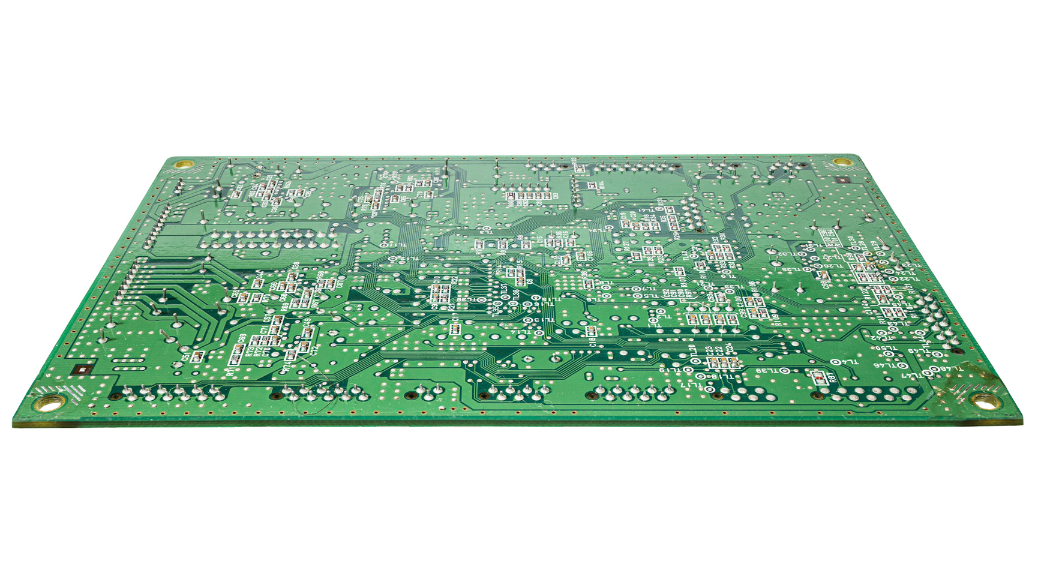
Why do some circuit boards fail early – even when the components themselves are spot-on? It’s often down to something that looks minor but matters a lot: PCB line spacing. If tracks sit too close together, especially in high-voltage or high-frequency circuits, you’re looking at possible shorts, interference, and heat issues. Not just design flaws – compliance failures too.
So, what’s the right distance between traces? And why does it matter across low- and high-voltage systems alike? Let’s break it down, starting with the safety side.
Preventing Electrical Short Circuits

So, the tighter the spacing between copper traces, the higher the risk – especially when moisture, voltage spikes, or board contamination come into play. This is where electrical spacing circuit board rules matter. It’s not just about neatness on the layout – it’s about safety in real conditions.
In high-voltage applications, too-narrow gaps can lead to arcing or breakdown between conductors. Even on low-voltage boards, poor spacing invites unexpected shorts, especially during thermal cycling or under physical stress.
Standards such as UL 796 and PCB standards IPC (like IPC-2221) lay out minimum clearance distances. For example, at 250V, you’re typically looking at 2.5mm spacing, though factors like altitude and pollution degree change the requirements.
Proper PCB line spacing stops fault chains before they begin – and that’s the first step to avoiding rework, warranty claims, or worse.
Managing Signal Integrity and Crosstalk
When signals start interfering with each other, or stray EMI sneaks in, the problem often points to layout – not components. In fact, signal integrity PCB layout issues tend to crop up more when traces are placed too close, especially in high-speed digital or RF designs.
It’s not just the voltage that matters – it’s rise times, impedance mismatches, and how well-separated your tracks are. Without enough PCB track separation, you’re inviting reflections, jitter, and unreliable data transfer.
The key? Consistent spacing and a grounded reference plane. Here’s a quick list of layout habits that support cleaner signals:
- Keep parallel high-speed traces apart to reduce crosstalk
- Use differential pairs where needed – but match spacing tightly
- Avoid sharp angles or length mismatches in fast paths
- Place decoupling capacitors close to power pins
So, signal quality starts well before a board hits production – it’s often set during layout spacing choices.
Compliance with Industry Safety Standards
Getting PCB line spacing right isn’t just good engineering – it’s a requirement. International safety standards clearly define how much clearance you need, depending on voltage, pollution level, and end-use environment.
For example, IPC-2221, part of the broader PCB standards IPC set, offers baseline figures. UL 796 applies to flammability and spacing for safety-critical applications. IEC 60950 adds further details for IT and telecom gear. These aren’t optional if your product goes near customers, medical equipment, or industrial power systems.
Here’s a simplified snapshot of minimum creepage and clearance PCB requirements for different voltage levels (assuming basic insulation, low pollution degree):
| Voltage (V) | Minimum Clearance (mm) |
| 30 | 0.13 |
| 100 | 0.6 |
| 250 | 2.5 |
| 400 | 4.0 |
Following these benchmarks helps prevent failures – and gives procurement and compliance teams what they need to sign off with confidence.
Ignoring spacing rules? That’s how testing labs send boards straight back.
Reducing Heat Build-Up Across Circuit Paths

It’s easy to focus on current ratings or copper weight, but heat dissipation in PCB design often hinges on spacing, too. When traces are packed too close, airflow is restricted and localised hot spots tend to form – especially in power sections or high-density layouts.
Wider spacing allows for better cooling, even if it’s passive. It also reduces the chance of thermal stress damaging the board over time. That’s particularly useful in designs with high duty cycles or environments where external cooling isn’t ideal.
So, while trace width gets the attention, PCB line spacing plays a quiet but vital role in keeping temperatures manageable – and failure rates low. It’s part of a balanced thermal strategy, not just an afterthought.
Enhancing Reliability and Product Lifespan
When boards fail early, the root cause isn’t always obvious – but poor PCB track separation is often part of the story. Over time, tight spacing can lead to dielectric breakdown, creeping contamination, or track delamination. Not instant failures – just slow, silent damage.
Spacing influences a board’s MTBF (mean time between failures), especially under variable loads or environmental stress. Even well-built boards can suffer if they’re pushed too hard, too close.
Take a board installed near an HVAC compressor. On paper, it passed all tests. In practice? Moisture ingress and high-voltage spikes led to arc marks and partial trace loss. Post-mortem pointed squarely at poor spacing.
So, the relationship is pretty clear: proper PCB line spacing is a long-term investment in reliability. Not just today’s performance, but tomorrow’s too.
How Professional PCB Layout Services Can Help
Getting spacing wrong is easy – especially under tight deadlines or when balancing dozens of layout rules. That’s why bringing in a professional PCB layout team early often saves time, money, and future headaches.
Altimex understands the tightrope between compliance, performance, and manufacturability. With in-house experts familiar with PCB standards IPC, UL, and IEC guidelines, your board isn’t just functional – it’s build-ready and audit-proof.
We factor in creepage and clearance PCB needs, signal integrity PCB layout, and heat dissipation in PCB design from the very first revision. Plus, with DFM (Design for Manufacturability) checks baked in, we help avoid spacing pitfalls that only show up at the fabrication stage.
It’s a straightforward approach: fewer revisions, more reliability. For more on layout support and PCB assembly, you can read about our PCB assembly capabilities or contact us directly.
Spacing might seem simple, but it plays a serious role in how well your board performs – and how long it lasts. From avoiding short circuits to staying within compliance, PCB line spacing affects safety, reliability, and efficiency at every level.
If you’re designing from scratch or updating an existing layout, spacing choices deserve early attention. Whether you’re revisiting specs or exploring how to customise a PCB board, every decision counts. Need help? Altimex brings layout precision, regulatory know-how, and manufacturability insight in one place. Start smarter – contact us early in the process.


