Printed Circuit Boards (PCBs) are the unsung heroes of modern electronics, supporting every device.
Tracing their history reveals innovation, from early conductor experiments to today’s intricate multilayer designs.
The history of printed circuit boards started in the 20th century when Charles Ducas and Paul Eisler separately conceived conductive pathways on insulating substrates, marking the PCB’s birth.
Over time, through-hole and surface mount technologies improved PCBs, offering compactness and reliability. Multilayer PCBs boosted component density and performance, advancing electronics.
This article explores PCB electronics evolution, printed circuit board history, and complex modern designs. Engineers and electricians will gain insights into these foundational components driving today’s technology.
What is a Printed Circuit Board?
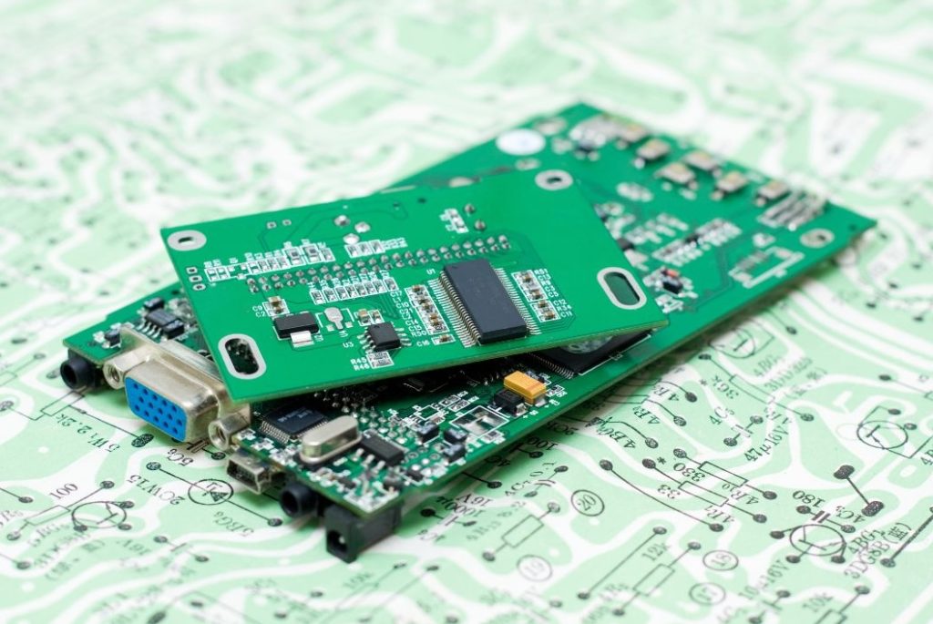
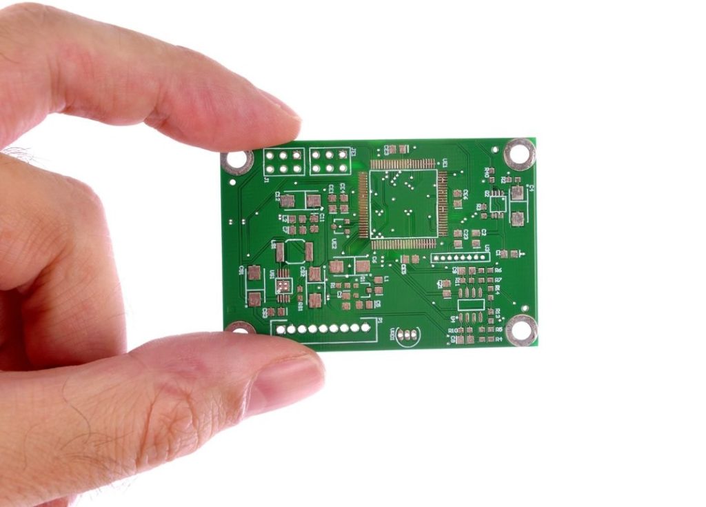
Printed Circuit Boards stand as pivotal components within electronic devices, serving as the foundation for connecting and supporting diverse electrical elements.
These boards comprise non-conductive substrates, typically composed of materials like fibreglass or epoxy, featuring intricately etched layers of conductive copper traces. PCBs play a vital role in facilitating the seamless flow of electrical signals among components, guaranteeing the precision and reliability of electronic devices.
Their significance lies not only in their connectivity function but also in their ability to provide a structured framework for mounting various electronic components, such as resistors, capacitors, and integrated circuits. This strategic arrangement optimises space utilisation, enhancing manufacturability and performance efficiency.
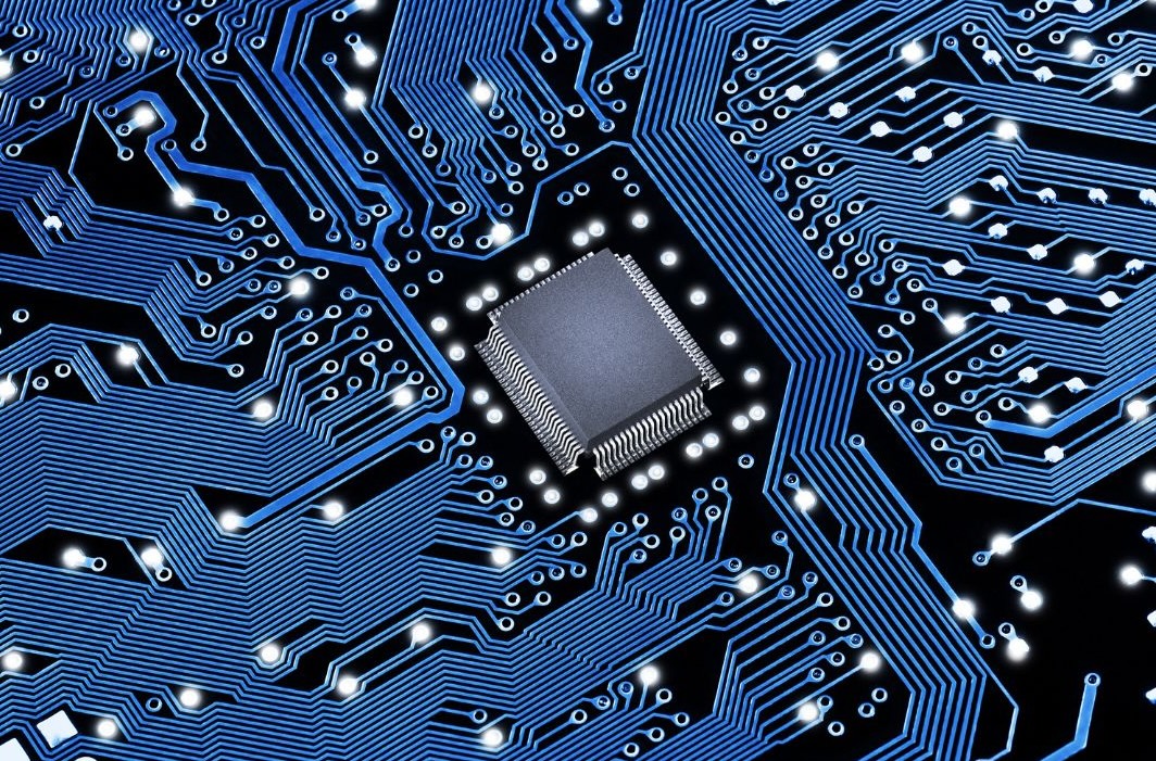
The PCB landscape encompasses designs that range from straightforward single-sided boards to intricate multilayered structures, tailored to the exacting requirements of the electronic system.
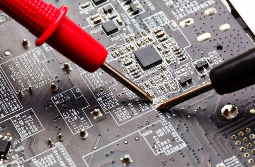
PCBs undergo a meticulous manufacturing process encompassing key stages such as etching, drilling, soldering, and assembly. This process yields customised boards, meticulously tailored to the specific demands and performance criteria of a wide array of applications.
Understanding the comprehensive journey of PCBs, from their humble beginnings to their current sophisticated designs, illuminates the core of modern electronics engineering. Engineers and electricians will gain valuable insights into the evolution and intricacies of these foundational electronic components.
Where are PCBs Used?
The evolution of PCBs is a testament to human ingenuity and technological advancement. Understanding their rich history and the stages of their design evolution is essential for engineers and electricians working across a multitude of industries. Here’s a breakdown of the key application areas and their impact on PCB design:
- Consumer Electronics: PCBs are the backbone of devices like smartphones, tablets, laptops, televisions, and gaming consoles, enabling compact and efficient designs.
- Automotive Industry: In vehicles, PCBs control engine units (ECUs), infotainment systems, navigation, and safety systems, demanding rugged and reliable PCB designs.
- Medical Devices: Diagnostic equipment, patient monitoring systems, and medical implants rely on PCBs for precision and reliability in critical healthcare applications.
- Aerospace and Defence: PCBs are integral to avionics, radar systems, satellite communications, and military equipment, where durability and performance under extreme conditions are paramount.
- Telecommunications: Routers, switches, modems, and base stations for wireless communication networks require PCBs to ensure seamless connectivity.
- Industrial Automation: PCBs play a crucial role in control systems for manufacturing processes, robotics, and instrumentation, enhancing efficiency and precision.
- Renewable Energy Systems: Solar inverters, wind turbine controllers, and battery management systems depend on robust PCB designs to harness renewable energy efficiently.
- Networking and IT Infrastructure: In data centres and telecommunications networks, PCBs are found in servers, switches, routers, and networking equipment, supporting fast and reliable data transfer.
- Consumer Appliances: PCBs are integral to household appliances like refrigerators, washing machines, air conditioners, and microwave ovens, improving functionality and efficiency.
- Wearable Technology: Smartwatches, fitness trackers, and other wearables rely on PCBs for compact designs and enhanced functionality, particularly in health monitoring and communication.
Early Developments of PCBs
The inception of PCBs dates back to the late 19th and early 20th centuries, with visionaries such as Albert Hanson pioneering experiments in conductive materials and electrical interconnection methods. However, it was the late 1800s work of Thomas Edison that laid the groundwork for the development of printed wiring technologies, a precursor to modern PCBs.
In Edison’s era, electrical systems were in their infancy, necessitating more efficient interconnection methods. His experiments with conductors and insulators were pivotal, leading to the emergence of printed wiring techniques.
From these early beginnings, PCBs have evolved into the intricate multilayer designs that drive contemporary electronic devices. This historical journey illustrates human ingenuity and engineering advancements.
Engineers and electricians can gain a deeper appreciation of PCB technology’s development, comprehending the intricate design principles and innovations responsible for shaping these fundamental components into the highly sophisticated elements vital to modern electronics.
Albert Hanson and Conductors
Albert Hanson, a Swedish engineer, played a pivotal role in the early evolution of PCBs.
In the late 1800s, Hanson made significant contributions to the development of conductive materials, a crucial aspect of modern PCBs. His experiments involved testing various metals and alloys to identify suitable conductors.
Hanson’s work was instrumental in refining techniques for depositing thin layers of conductive materials onto insulating substrates, a foundational step in modern PCB manufacturing.
Notably, his research highlighted the effectiveness of materials like copper and silver in transmitting electrical signals, a fundamental requirement for PCBs. Additionally, his exploration of different conductive materials contributed to advancements in electrical conductivity and resistance, critical factors in PCB design and performance.
Hanson’s innovative approaches to conductor materials and manufacturing techniques set the stage for subsequent PCB technology developments, profoundly influencing the evolution of electronic devices and systems. Engineers and electricians today can trace the roots of modern PCBs back to Albert Hanson’s pioneering work.
Thomas Edison and PCBs
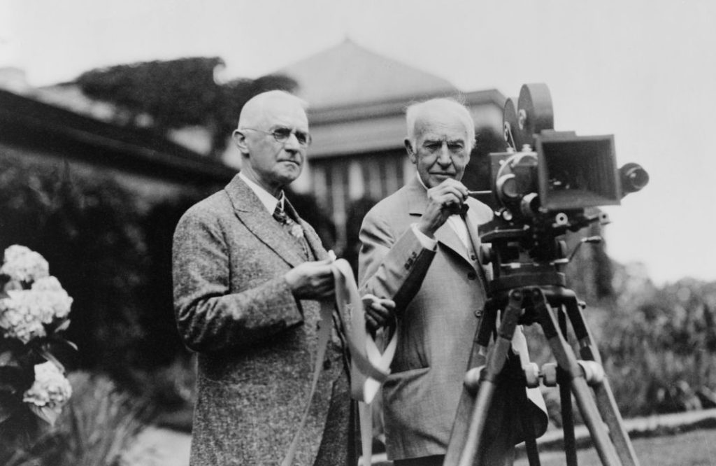
Thomas Edison, a luminary in electrical engineering during the late 19th century, left an indelible mark on the field, laying the groundwork for the eventual evolution of Printed Circuit Boards.
Edison’s pioneering experiments with various electrical conductors and insulators significantly contributed to our understanding of electricity’s behaviour.
Of particular importance was Edison’s development of techniques to insulate electrical wires. By employing materials like silk threads, he safeguarded wires against short circuits, a concept foundational to PCB design.
While not directly tied to PCBs, Edison’s groundbreaking invention of the phonograph in 1877 exemplified his innovative spirit, inspiring future inventors and engineers to explore new technologies.
Edison’s inventions and advancements in electrical engineering played a pivotal role in society’s industrialisation, fostering an environment ripe for technological innovations, including those related to electronic circuitry.
Although PCB technology emerged decades after Edison’s time, his legacy as an inventor and innovator set the stage for subsequent developments in electrical engineering, including the sophisticated designs of modern-day printed circuit boards.
Engineers and electricians today continue to benefit from the pioneering spirit that Edison exemplified.
PCB Precursors
The road towards the sophisticated PCBs we rely on today is a tale of innovation and evolution. Before the advent of modern PCBs, various precursors laid the groundwork for their development.
Early forms of electrical interconnection included point-to-point wiring, where components were manually connected with wires. Another precursor was the use of “breadboards” – temporary platforms for circuit testing, where components were inserted into holes on a board and connected with wires.
Albert Hanson’s work in the late 1800s, pioneering the development of conductive materials, played a pivotal role in shaping PCB technology. His contributions paved the way for more organised and efficient circuit designs.
In the early 20th century, flat metal plates with engraved circuit patterns emerged as precursors to modern PCBs. However, these early designs were often handmade and lacked the sophistication of today’s mass-produced boards.
The rise of radio technology in the early 20th century spurred advancements in circuit board design, leading to refined methods for creating complex and reliable electrical connections.
This marked a significant step towards the PCBs we know today, highlighting the continuous evolution and innovation that have shaped the world of electronics.
Engineers and electricians today benefit from this rich history, understanding the foundations upon which modern PCB design stands.
Early designs of PCBs
The War and PCB Advancements
The history of the printed circuit board in its current sophisticated state is deeply intertwined with the tumultuous backdrop of World War II.
This period catalysed momentous advancements in PCB technology, responding to the escalating demand for dependable electronic systems, particularly in military applications.
The exigencies of war drove the development of radar systems and communication equipment, necessitating compact and reliable circuitry. This imperative led to notable innovations in PCB design and manufacturing, shaping their future.
In particular, the need for lightweight and robust electronic components for aircraft and military vehicles prompted the adoption of PCBs over traditional point-to-point wiring methods, streamlining complex electrical systems.
Furthermore, military research and funding during and after the war accelerated the refinement of PCB materials. Epoxy laminates and copper foils emerged, engineered to withstand the harshest environments and combat conditions.
The invaluable knowledge and expertise gained during these wartime PCB advancements laid the foundation for the rapid expansion of PCB technology in post-war civilian industries.
This legacy has perpetuated innovation in electronics manufacturing for decades, underlining the pivotal role of PCBs in modern engineering. Engineers and electricians today owe much of their field’s progress to the crucible of World War II, where PCBs truly came of age.
The Integrated Circuit
The transformation of Printed Circuit Boards to their modern state hinged on the late 1950s breakthrough—the integrated circuit (IC). This innovation revolutionised PCB technology, enabling the integration and miniaturisation of electronic components onto semiconductor chips.
ICs played a pivotal role in streamlining PCB designs, housing entire circuits within a single chip, yielding more compact and efficient layouts. This integration also ushered in substantial enhancements in electronic device performance, reliability, and energy efficiency.
In response, PCB designs adapted to meet the unique needs of ICs, incorporating specialised layouts for mounting and connecting these miniature components.
The widespread adoption of ICs ignited a surge in PCB technology innovation, fueling the development of advanced electronic systems.
Today, engineers and electricians witness the enduring impact of this milestone in PCB history—a transformative shift that forever reshaped electronic circuitry, enhancing efficiency and capabilities.
The Evolution of PCB Technology
Introducing Double-Sided PCBs
Double-sided PCBs mark a significant stride in PCB technology, ushering in more intricate circuit designs and heightened component density.
These boards boast conductive traces on both sides of the substrate, enabling interconnections between components on both the top and bottom layers. This innovation expanded the horizons of electronic device design, accommodating a greater number of components within a compact form factor.
Consequently, it facilitated the creation of advanced electronic devices, elevating functionality and performance across multiple industries. Today, double-sided PCBs find common applications in sectors requiring elevated circuit density, including telecommunications equipment, industrial controls, and automotive electronics, contributing to the continuous evolution of electronic engineering.
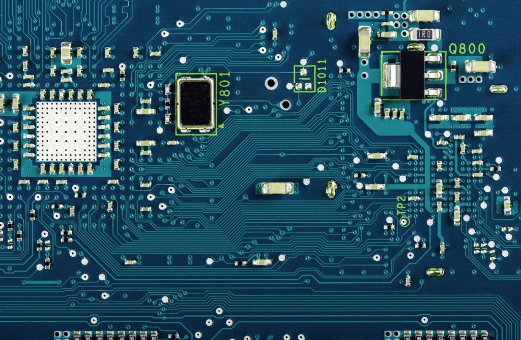
Multilayer PCBs
Multilayer PCBs represent a significant leap in PCB evolution, enabling intricate and compact electronic designs through the stacking of multiple layers of conductive and insulating materials.
By incorporating numerous signal layers, power planes, and ground planes, they enhance signal integrity, reduce electromagnetic interference (EMI), and improve thermal management. This technological advancement has revolutionised the electronics industry by facilitating the integration of more components into smaller form factors, leading to the miniaturisation of electronic devices.
Engineers benefit from greater design flexibility, enabling advanced features like high-speed signal routing, impedance matching, and controlled impedance traces.
The evolution of multilayer PCB fabrication techniques, materials, and manufacturing processes ensures increased reliability, cost-effectiveness, and scalability in producing complex electronic systems.
Surface Mount Technology
Surface Mount Technology (SMT) stands as a transformative milestone in PCB design, revolutionising the landscape by enabling direct component mounting onto the board’s surface, eliminating the need for through-holes.
These SMT components, smaller and lighter than their through-hole counterparts, permit higher component density and electronic device miniaturisation.
SMT’s introduction brought about enhanced manufacturing efficiency and reduced production costs, thanks to automated assembly processes and heightened production throughput. The flexibility in component placement and routing that SMT affords facilitated the creation of advanced PCB designs, including multilayer boards.
Today, SMT reigns supreme in PCB assembly, driving continuous innovations in electronics manufacturing. It empowers the creation of smaller, lighter, and more potent electronic devices, marking a pivotal chapter in PCB evolution.
PCBs in Fibre Optic Cable Manufacturing
PCBs have evolved significantly to meet the exacting demands of fibre optic cable manufacturing.
They transitioned from traditional rigid substrates to flexible and hybrid materials, adept at accommodating intricate designs. This evolution involves material science advancements, including specialised substrates with high thermal stability, low dielectric loss, and impeccable mechanical properties to ensure reliable performance in harsh environments.
Miniaturisation and component densification on PCBs have been instrumental in optimising the footprint of fibre optic cable assemblies, resulting in compact and lightweight designs suitable for space-constrained applications.
Multilayer PCBs with embedded passive components and high-density interconnects have gained prevalence in fibre optic cable manufacturing, enabling efficient signal routing, improved signal integrity, and heightened reliability.
Advanced fabrication techniques, such as laser drilling, precision etching, and automated assembly, have revolutionised PCB production for fibre optic cable manufacturing, allowing cost-effective mass production while maintaining stringent quality standards.
For further in-depth knowledge and expert guidance on the evolution and intricacies of Printed Circuit Boards, we invite you to reach out to Altimex.
Our team of specialists is dedicated to providing comprehensive insights into PCB technology and working directly with the cutting-edge developments that shape its design today.
Whether you are an engineer seeking to stay at the forefront of PCB innovation or an electrician aiming to enhance your understanding of these fundamental components, Altimex is your trusted partner, so contact us now to explore the vast world of PCBs and unlock new horizons in electronics.