

Understanding how PCB assembly works means understanding where projects succeed or fail. It is not just a sequence of steps, it is a controlled process where early decisions affect cost, timelines, and long-term reliability.
Design choices influence manufacturability, material and component selection affect performance and availability, assembly methods define density and durability, and testing confirms whether the board works as intended before it reaches your product.
This guide breaks down each stage in the PCB assembly process and explains what matters in practice, not just in theory.
Every PCB Assembly Project Starts With Design Review
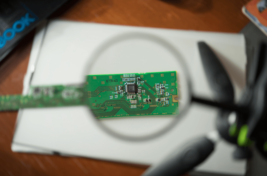
Design for manufacture (DFM) ensures your PCB can be built reliably, not just function on paper.
Before production starts, engineering and manufacturing teams review the design to identify risks. This is where many issues are prevented rather than fixed later at a higher cost.
Key checks include:
- Layout spacing and trace routing against manufacturing tolerances
- Component placement for accessibility and assembly flow
- Thermal considerations and heat dissipation paths
- Pad geometry and solder joint compatibility
- Drill sizes and layer stack feasibility
In practice, problems at this stage often come from designs that push density without considering assembly limits. Tight spacing or poor placement can lead to solder defects or rework.
A clear, manufacturable design improves yield, reduces delays, and stabilises the entire PCB manufacturing process.
Scale Your Production
From prototype to full-scale electronic assembly, our UK facility is equipped to handle your requirements.
Get a QuoteMaterial and Component Selection Shape the Build
Material and component choices directly affect performance, durability, and lead times.
Substrate selection, such as standard FR-4 or specialist laminates, determines:
- Signal integrity
- Thermal resistance
- Environmental durability
Component selection adds another layer of complexity. Package types, electrical ratings, and lifecycle status all influence reliability.
In real projects, availability is often the deciding factor. A high-spec component is not useful if it introduces a 20-week lead time or risks obsolescence mid-production.
Typical trade-offs include:
- Lower cost materials vs long-term reliability
- Compact components vs assembly complexity
- High performance parts vs sourcing risk
Strong decisions here balance engineering requirements with realistic supply conditions within the PCB production process.
Procurement Keeps the Project Moving
Procurement is where many PCB projects lose time.
Even with a complete design, production cannot start without the right materials and components in place. Delays here quickly cascade into missed deadlines.
Key procurement risks include:
- Component shortages in global supply chains
- Counterfeit or non-compliant parts
- Long lead items delaying production
- Price volatility affecting budgets
In practice, the biggest issue is poor visibility. If sourcing risks are not identified early, projects stall unexpectedly.
Experienced manufacturers plan procurement alongside design, not after it. This reduces disruption and keeps the electronics assembly process aligned with delivery targets.
Engineering-Led Solutions
Work with a team that understands modern electronics and end-to-end manufacturing.
Our ExpertiseSurface Mount and Through Hole Assembly Bring the Board to Life
Assembly is where the PCB becomes a working circuit.
Two main methods are used:
Surface Mount Technology (SMT)
Components are placed directly onto the board surface using automated machines. Reflow soldering secures them in place.
Best suited for:
- High-density designs
- Small components
- Automated, high-volume production
Through Hole Technology (THT)
Component leads are inserted into drilled holes and soldered on the opposite side.
Best suited for:
- Connectors and large components
- Applications with mechanical stress
- Products requiring stronger physical bonds
Key differences:
- Surface mount supports compact layouts and speed
- Through hole provides mechanical strength
- Surface mount enables higher circuit density
- Through hole improves durability in harsh conditions
Most modern designs use a combination of both. The right choice depends on performance requirements, not just cost, especially in surface mount vs through hole decisions.
Soldering Quality Has a Major Impact on Performance
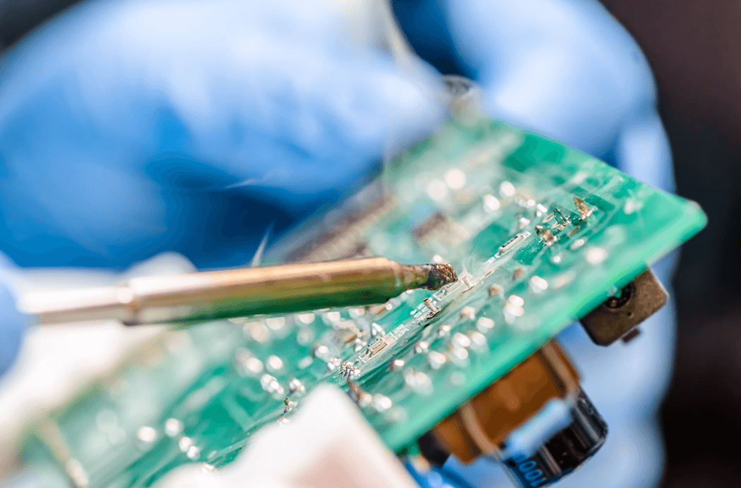
Soldering is a critical point of failure if not controlled properly.
It creates both the electrical connection and the mechanical bond between components and the PCB. Weak solder joints lead to intermittent faults that are difficult to diagnose after deployment.
Common defects include:
- Cold joints causing poor conductivity
- Solder bridges creating short circuits
- Voids reducing strength and heat transfer
These issues are rarely random. They usually result from inconsistent process control, such as incorrect temperature profiles or poor solder paste application.
Reliable soldering supports long-term performance. Poor soldering often leads to field failures, not immediate defects, making it more costly to resolve.
Ready to start your project?
Contact our technical team today to see how Altimex can streamline your electronics supply chain.
Contact UsInspection and Testing Confirm Everything Works as Intended
Inspection and testing ensure that defects are identified before the board reaches your product.
Different methods are used depending on complexity:
- Automated Optical Inspection (AOI) detects placement and visible solder issues
- X-ray inspection checks hidden joints, such as ball grid arrays
- Functional testing confirms the board operates under real conditions
Catching defects early reduces rework and prevents faulty units moving further through production.
In practice, insufficient testing is a common cost-saving mistake. It reduces upfront cost but increases the risk of failure later in the product lifecycle.
Strong PCB testing and inspection processes protect both performance and reputation.
For a deeper breakdown, see our guide to the PCB assembly process.
Quality Control Supports Consistency at Every Stage
Quality control is not a single step. It runs throughout the entire process.
It monitors:
- Material consistency
- Assembly conditions
- Inspection results
Standards such as IPC-A-610 define acceptable quality levels for electronic assemblies, while ISO 9001:2015 supports structured process control.
In real-world production, variation is the main risk. Without consistent monitoring, small deviations lead to larger defects over time.
Traceability is also critical. Being able to link each board to its materials and processes allows issues to be identified and corrected quickly.
Consistent quality control supports repeatability, which is essential for scaling production.
Final Assembly and Packaging Prepare Boards for Delivery
Once the PCB is complete, final assembly may integrate it into a larger system.
This can include:
- Additional wiring
- Mechanical components
- Enclosures
Final checks confirm that all specifications have been met before dispatch.
Packaging is equally important. PCBs are sensitive to:
- Electrostatic discharge (ESD)
- Mechanical shock
- Environmental conditions
Anti-static materials and protective packaging reduce risk during transport.
Projects involving flexible PCB assembly require additional care due to material flexibility and handling sensitivity.
Communication and Planning Help Keep Delivery on Track
Clear communication between the client and the manufacturer reduces delays and avoids costly mistakes.
Projects often run into issues when:
- Design changes are not communicated early
- Lead times are not aligned with expectations
- Volume changes are introduced late
Regular updates across design, procurement, and production stages help keep everything aligned.
In practice, the most successful projects involve early collaboration. Aligning requirements before production starts reduces rework and improves delivery confidence.
If you are planning a PCB project and want to reduce risk at each stage, contact us to discuss your requirements.