
In electronic design and production, the thickness of a PCB significantly affects both the functionality and the durability of the final product.
The right thickness is needed for the success of electronic devices.
In this article, we’ll guide you through the selection process, step-by-step, ensuring your design matches both project requirements and industry standards.
For newcomers or those seeking a refresher, why not first read our cover-all guide to how PCBs work, before revisiting here for more.
What is PCB Thickness?
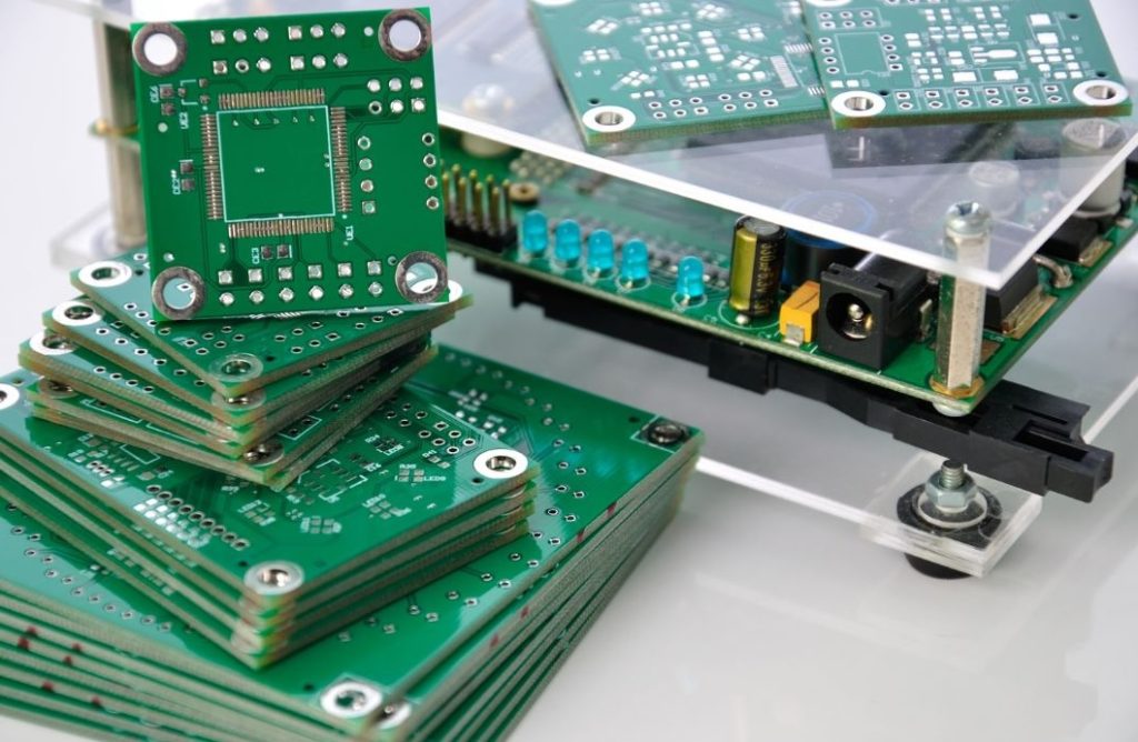
When discussing PCB thickness, we are discussing the width of the core board, typically measured in millimetres or inches.
Standard thicknesses range from 0.8mm to 1.6mm, tailored to meet specific design needs.
The choice of thickness impacts other design parameters like board size and complexity, influencing the device’s application and performance from structural integrity to thermal management.
Step-by-Step Guide to Choosing PCB Thickness
1. Define Your Project’s Technical Requirements
The first step in determining the ideal PCB thickness involves documenting technical specifications such as voltage and current requirements, which dictate the PCB’s robustness.
Systematic documentation and review of these specifications are needed, particularly in complex or unfamiliar projects.
Consultation with experienced electrical engineers is advisable to avoid costly design mistakes.
2. Assess Mechanical and Environmental Constraints
PCBs must endure mechanical stresses and environmental factors such as temperature and humidity.
For example, PCBs in automotive applications may need greater thickness to withstand vibrations and thermal cycles.
Evaluating the installation environment and performing tests under simulated conditions are needed to understand how different thicknesses might cope in actual scenarios.
3. Determine the Optimal Layer Count
The PCB board thickness is influenced by the number of layers required for the circuit. Increasing the layer count enhances complexity and functionality but may require thicker PCBs to accommodate additional conductive layers and isolation needs.
Collaboration with layout designers is essential to optimise layer distribution for both thermal and mechanical performance.
4. Consider Thermal Management Requirements
Thermal management is especially useful in compact or high-power devices where excess heat can impair functionality.
The PCB’s thickness affects its heat dissipation capabilities.
Thicker boards, while structurally sound, might necessitate the use of high thermal conductivity materials like Aluminium to manage heat effectively.
5. Consult Industry and Safety Standards
Following industry standards, such as those from the IPC, is required for determining suitable PCB thickness.
These standards allow for safety and functionality, easing compliance during audits and certifications.
Keeping abreast of the latest standards so that designs meet all required guidelines.
6. Factor In Manufacturing Capabilities and Costs
The chosen thickness affects both manufacturing processes and costs. Thicker PCBs may incur higher material and production costs during any PCB assembly.
Early consultation with manufacturers can reveal the feasible thicknesses their equipment can handle efficiently, aiding in cost-effective design decisions. For more details, explore electronic manufacturing capabilities.
7. Decide on Material Types and Their Thickness Availability
The material choice affects PCB thickness availability.
Materials like FR-4 offer various thicknesses, suitable for many applications, whereas others like CEM-1 may have limitations.
When selecting the optimal PCB thickness, consider material properties like thermal stability and mechanical strength.
8. Prototype Testing
Testing prototypes is needed to validate thickness decisions. It allows observations of how thickness influences PCB performance in real-world conditions, enabling necessary adjustments before final production.
Thermal cycling and stress tests are valuable methods for assessing different thicknesses’ resilience.
9. Finalise Thickness Based on Test Results and Feedback
Using feedback from testing to finalise PCB thickness is required.
This process helps refine thickness choices based on practical data and input from stakeholders, ensuring a balance between cost, performance, and manufacturability.
10. Plan for Future Scalability and Updates
Considering future scalability and updates at the design stage saves time and resources.
Designing with flexibility for technological advancements or application changes means that the PCB remains relevant and adaptable.
Regular revisions as new technologies emerge enhance the product’s lifecycle.
Key Factors Affecting PCB Thickness
Here are some key factors to consider when designing and being conscious of any thickness of a PCB.
Number of PCB Layers
- More layers typically require increased thickness to accommodate additional circuitry.
- Layer count affects electrical isolation and signal integrity, influencing thickness decisions.
- Consider the purpose and complexity of the PCB when deciding on the layer count and corresponding thickness.
Signal Type
- Thickness needs vary between digital and analogue signals due to differences in signal integrity requirements.
- High-speed digital signals may require thicker PCBs to reduce electromagnetic interference (EMI).
- Analogue signals benefit from stable environments provided by appropriate PCB thickness to minimise noise.
Material Selection
- Choose materials based on required thickness and performance characteristics like thermal resistance and dielectric constant.
- Material rigidity and durability also influence the minimum and maximum thickness that can be effectively used.
- Assess the compatibility of material properties with the intended electrical and mechanical demands of the PCB.
Operating Environment
- Design to withstand specific environmental conditions such as high temperatures, humidity, or corrosive atmospheres.
- Consider the mechanical loads and stresses the PCB will face, which may need a thicker board.
- Environmental resistance often dictates the use of specific materials and thicknesses for longevity and reliability.
Copper Thickness
- Copper weight affects overall PCB thickness and is needed for current carrying capacity and thermal management.
- Thicker copper layers are often required for high-power applications to handle increased current without overheating.
- The choice of copper thickness must balance electrical performance needs with physical PCB dimensions and weight constraints.
Special Requirements
- Flexibility Needs: For applications requiring flexible PCBs, such as wearable technology, the thickness must allow for bending without damage. Opt for thinner, more pliable materials to meet these needs.
- Impedance Control: Critical for maintaining signal integrity in high-speed designs. Thickness and material choices must align with impedance specifications to prevent signal loss or distortion.
- High-Frequency Performance: Specialized PCBs like those used in RF (Radio Frequency) applications often require specific thicknesses to minimise electromagnetic interference and optimise performance.
Choosing the right PCB thickness is needed for the best performance and cost-efficiency.
By considering all discussed factors, designers can improve the durability and functionality of their electronic devices.
Keeping up with new materials and technologies means that your PCB designs and builds are both competitive and effective.