The PCB assembly process is where a bare circuit board becomes a working electronic product, so design data turns into something that can be powered, tested and installed.
For many teams, this stage can feel a little unclear at first, that is because several closely linked steps must happen in the right order. Engineers, product managers and procurement teams often want clarity on how PCB assembly works before committing to production, so expectations around quality, timing and risk feel grounded rather than optimistic.
In practice, assembly involves more than placing parts and melting solder, so preparation, inspection and testing shape the final outcome just as much as machinery does. Each stage builds on the one before it, so accuracy early on usually leads to fewer delays later.
When managed by an experienced UK manufacturer, the PCB manufacturing process feels controlled, traceable and predictable, which matters when performance and reliability cannot slip.
Design Validation and Data Preparation
Every PCB assembly process begins with data validation, so no physical work starts until the information is confirmed. Gerber files, CAD data and drawings are reviewed, which allows layer alignment, pad dimensions and track details to be checked. The bill of materials is verified at the same time, so part numbers, quantities and approved alternatives match what will actually be placed on the board.
Manufacturability checks often follow, so potential issues like unclear footprints or tight tolerances are identified early. Pick and place data is then prepared, which tells machines where each component should sit and how it should be oriented. Strong preparation at this stage usually prevents errors from travelling downstream, saving time and avoiding avoidable rework.
Solder Paste Application
Once the data is approved, assembly moves into solder paste application, so each pad receives a controlled amount of solder. A stencil is aligned over the PCB, and paste is applied through accurately sized apertures. This step sets the foundation for joint quality, even though its impact is sometimes underestimated.
If paste volume or alignment drifts slightly, defects can appear later, so solder bridges, weak joints or incomplete connections become more likely. Careful stencil design, clean printing and regular checks help keep this stage consistent, so later processes begin on stable ground.
Component Placement

After paste printing, components are placed using automated pick and place machines, so speed and accuracy remain high even with very small surface mount parts. These systems handle fine pitch components with tight tolerances, which demand precise calibration and verification.
Several factors influence placement quality, including:
- Component packaging and feeder condition
- PCB support and flatness
- Machine calibration and alignment accuracy
- Verification checks before reflow
This stage defines much of the SMD assembly process, so close control here reduces rework and improves overall yield.
Reflow Soldering
With components positioned, the board enters reflow soldering, so heat melts the solder paste and forms electrical joints. The PCB passes through a reflow oven with a controlled temperature profile that increases heat gradually rather than abruptly. This protects components from thermal shock and allows solvents in the paste to evaporate safely.
At peak temperature, the solder melts and wets the pads and component leads, forming strong joints. Controlled cooling then solidifies the solder, locking parts in place. A stable reflow soldering process supports joint strength and long-term reliability, which is why temperature control matters at this stage.
Through-Hole Soldering
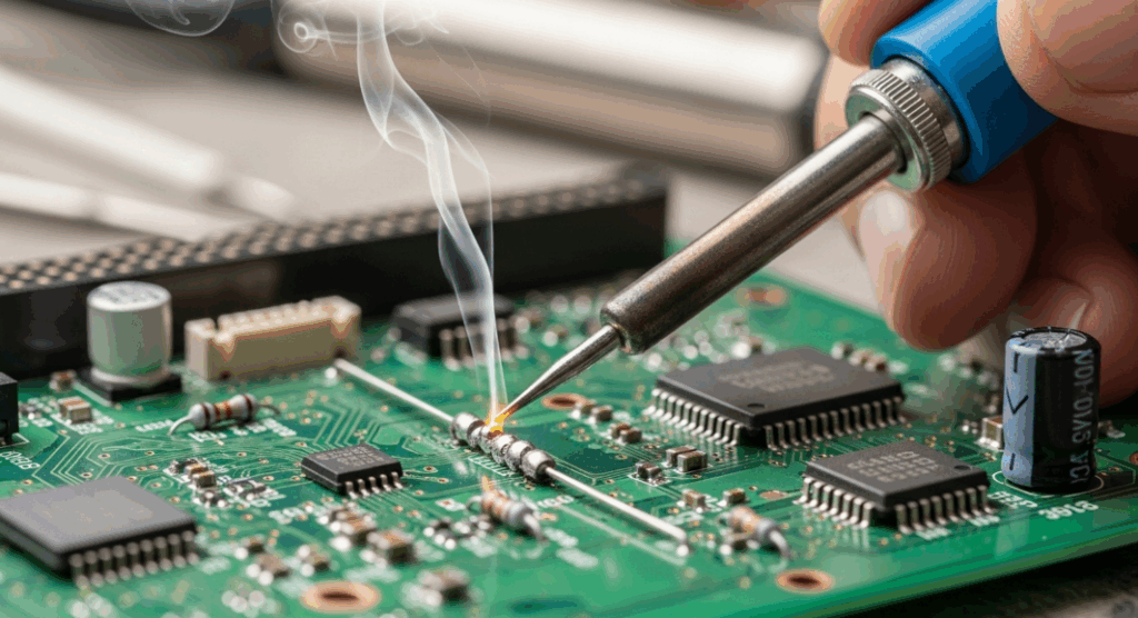
Some designs include components that cannot be surface-mounted, so through-hole assembly steps follow reflow where required. These parts pass their leads through drilled holes, providing strong mechanical support for connectors, large capacitors and heavier components. Soldering may be completed by hand or by wave soldering, depending on volume and design.
This stage is more labour-intensive, so workmanship plays a larger role in quality. Careful solder control helps avoid cold joints and excess solder, ensuring both electrical performance and mechanical strength meet expectations.
Automated Optical Inspection
Inspection begins soon after soldering, so defects are identified before further value is added. Automated optical inspection uses cameras to compare each board against a known reference, checking solder joints, component presence, polarity and alignment.
AOI is effective at catching visible defects early, so rework can happen before testing or final assembly. In some cases, X-ray inspection is used, allowing hidden joints beneath larger packages to be assessed. This stage forms an important part of PCB inspection and testing, supporting consistent quality across production runs.
Functional and Electrical Testing
Visual inspection alone is not enough, so electrical testing confirms that assemblies behave as intended. Tests may include continuity checks, in circuit testing or functional testing, depending on the product. Power and signals are applied, which verifies connections, component values and basic operation.
Testing reduces the risk of field failures, so issues are identified under controlled conditions rather than after deployment. For many teams, this step confirms that the PCB production stages have delivered both accuracy and dependable performance.
Final Assembly and Quality Approval
The final stage prepares assemblies for dispatch, so additional items like cables, housings or sub-assemblies may be fitted if required. A full visual check confirms cleanliness, labelling and overall finish, ensuring the assembly meets agreed standards. Documentation and certification are added where necessary, so traceability remains intact.
Many organisations prefer working with a supplier that offers complete PCB assembly board services, like us here at Altimex, so design intent is preserved through to delivery.
If you want to discuss requirements, timelines or testing expectations, you can contact us directly to align everything early and avoid unnecessary delays.


