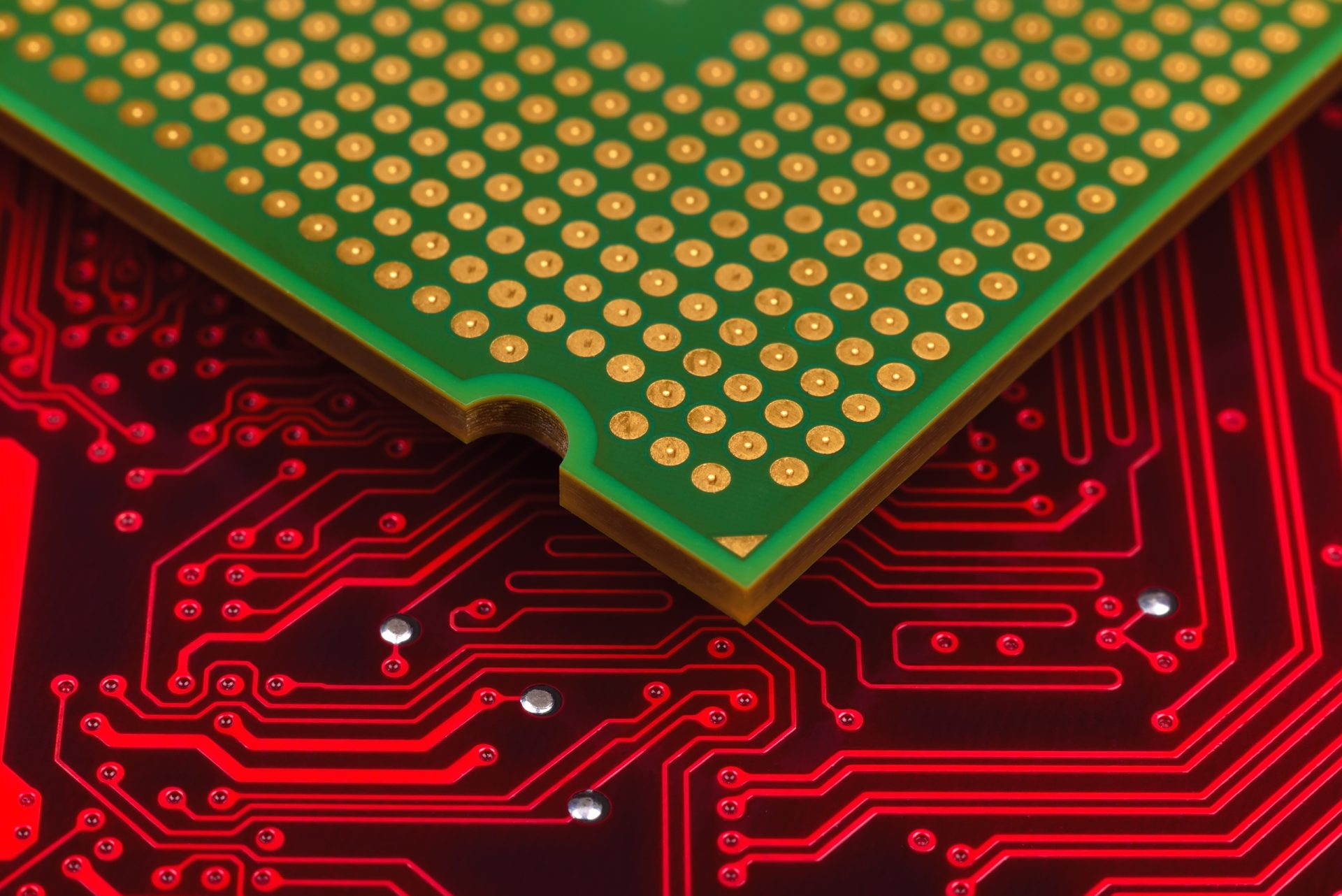
Printed Circuit Boards (PCBs) are the backbone of modern electronic devices, providing the platform that supports and connects essential components. With roots tracing back to the early 20th century, PCB layers have evolved significantly, transforming from simple single-layer boards to the complex multi-layer systems that power today’s advanced technology.
This guide delves into the intricate world of PCB layers, exploring their development, structure, and essential role in device performance and reliability.
Whether you’re an engineer, PCB designer, or electronics enthusiast, mastering the nuances of these layers is crucial for successful PCB design.
Basic Structure of a PCB
PCBs typically consist of several distinct layers, each with a specific function that contributes to the overall performance of the board. The primary layers include:
- Substrate: Provides structural support and determines the board’s rigidity.
- Copper Layers: Facilitate electrical conductivity.
- Solder Mask: Protects copper layers from oxidation and prevents short circuits.
- Silkscreen Layer: Used for labelling components and assisting with assembly and troubleshooting.
Together, these layers form a cohesive structure that enables the PCB to operate efficiently in various electronic devices.
Types of PCB Layers
Single-Layer PCBs
Single-layer PCBs feature one layer of conductive material, typically copper, on one side of the board. These are the simplest type of PCBs, commonly used in straightforward electronic devices due to their lower cost and ease of manufacturing. Applications include calculators, radio equipment, and printers.
Double-Layer PCBs
Double-layer PCBs have conductive material on both sides of the substrate, allowing for more complex circuitry. This design offers increased flexibility and the ability to incorporate more components, making it suitable for industrial controls, automotive electronics, and amplifiers. The key difference between double-layer and multi-layer PCBs lies in the number of conductive layers, balancing complexity and cost.
Multi-Layer PCBs
Multi-layer PCBs consist of three or more layers of conductive material, providing the capacity for highly complex and dense circuitry. These PCBs are essential in advanced applications such as computers, medical equipment, and aerospace technology, offering improved performance and support for intricate designs.
Multi-layer PCBs offer superior performance and design complexity, making them ideal for advanced technology. However, single and double-layer PCBs are more cost-effective for simpler applications.
Composition of PCB Layers
Substrate Materials
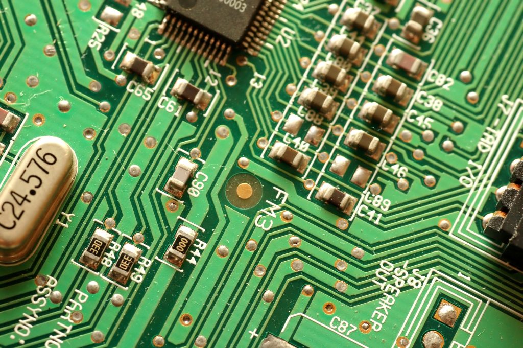
The substrate is the base material of the PCB, providing structural integrity and electrical insulation. Common substrates include FR4, a durable and widely-used material known for its excellent balance of cost and performance. The choice of substrate can significantly impact thermal stability, mechanical strength, and overall cost. For instance, while FR4 is cost-effective, materials like polyimide offer better thermal resistance but at a higher price.
Copper Layers
Copper layers are crucial for conducting electricity within the PCB. The thickness of these layers varies based on the current-carrying requirements and is applied through electroplating or lamination. Thicker copper layers enhance the board’s ability to handle higher currents, making them essential in high-power applications.
Solder Mask
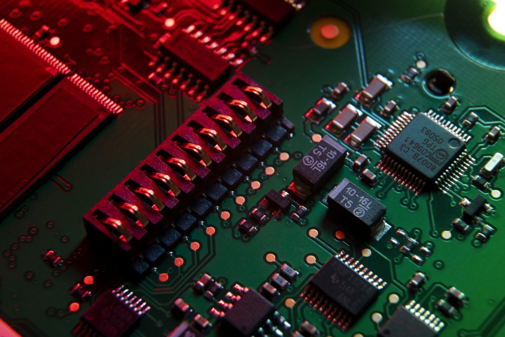
The solder mask is a protective layer applied over the copper traces to prevent oxidation and short circuits. Typically made from epoxy-based polymers, the solder mask is most commonly green but can be found in other colours. This layer is essential for protecting the copper from environmental damage and ensuring the integrity of the soldering process.
Silkscreen Layer
The silkscreen layer is used for labelling components, test points, and other essential information on the PCB. It plays a critical role in assembly and troubleshooting by providing clear visual indicators for component placement and orientation. Common materials for silkscreen include epoxy ink, usually white, to contrast with the solder mask.
Functions of Each PCB Layer
Conductive Pathways
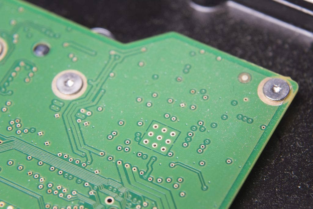
Conductive pathways are formed by copper traces, enabling the flow of electrical current between components. The design of these pathways is crucial, as improper design can lead to PCB issues such as signal loss and interference. Key factors in pathway design include trace width, spacing, and overall layout.
Insulation
Insulation within the PCB is provided by the substrate and the solder mask, both of which prevent electrical shorts by isolating the copper layers. Different insulating materials offer varying levels of thermal and electrical resistance, directly impacting the board’s performance.
Component Mounting
Component mounting techniques, such as Surface-Mount Technology (SMT) and Through-Hole Technology (THT), are critical for attaching electronic components to the PCB. Recent innovations in SMT, including the use of smaller components and higher-density placements, have significantly improved manufacturing efficiency and product performance. Proper mounting is essential for ensuring the reliability and longevity of the PCB.
Manufacturing Process of PCB Layers
Design and Layout
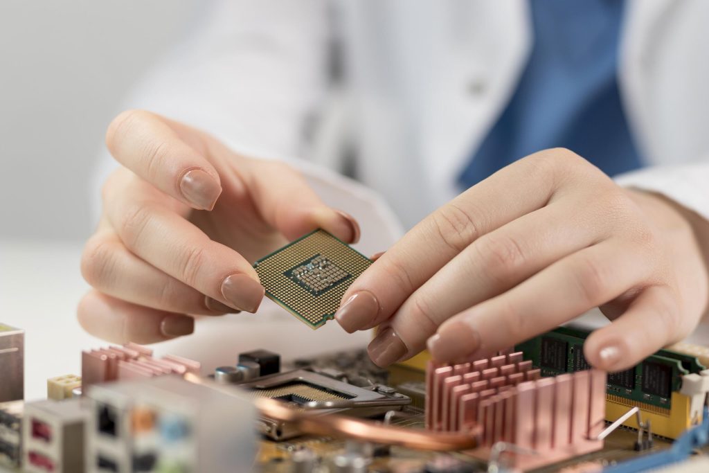
This phase of designing a PCB layout is critical in the PCB manufacturing process, involving the careful planning of the board’s structure and circuitry. Tools like CAD software are used to create detailed layouts that determine the placement of components and conductive pathways. Accurate design is vital for ensuring the PCB meets its intended specifications and functions correctly.
Lamination and Etching
Lamination involves bonding multiple layers of the PCB together using heat and pressure, followed by etching to remove unwanted copper and form the desired circuit patterns. Precision in these steps is crucial, as any errors can compromise the integrity of the conductive pathways.
Drilling and Plating
Drilling is used to create holes in the PCB for component leads and vias, which connect different layers. These holes are then plated with copper to form conductive pathways. The accuracy of drilling and plating is essential for the PCB’s overall performance.
Assembly and Testing
The PCB assembly process involves placing and soldering components onto the board, followed by rigorous testing to ensure the product functions as intended. Common testing methods include visual inspection, automated optical inspection (AOI), and functional testing.
Importance of Layer Stackup
Signal Integrity
Layer stackup plays a vital role in maintaining signal integrity by influencing the electromagnetic environment of the PCB. Proper stackup design can minimise signal interference, ensuring high-quality signal transmission. Techniques such as the careful arrangement of layers and the use of ground planes are commonly employed to preserve signal integrity.
Thermal Management
Effective thermal management is crucial for preventing overheating and extending the lifespan of PCB components. Innovations in this area, such as the use of thermal vias, advanced heat sink materials, and improved layer arrangements, have greatly enhanced heat dissipation in modern PCBs.
Minimising Crosstalk
Crosstalk, or signal interference between adjacent traces, can severely impact the performance of a PCB. Minimising crosstalk involves careful trace routing and maintaining adequate spacing between conductive pathways. Techniques like using differential pairs and implementing shielding can effectively reduce crosstalk.
Common Issues with PCB Layers
Delamination
Delamination occurs when layers of the PCB separate, often due to thermal stress or manufacturing defects. This issue can lead to electrical failures and reduced mechanical strength. Preventing delamination involves using high-quality materials and adhering to proper manufacturing techniques.
Short Circuits
Short circuits in PCBs are typically caused by unintended connections between conductive pathways. Common causes include solder bridges, manufacturing defects, and physical damage. Preventing short circuits requires careful design, meticulous soldering techniques, and thorough inspection.
Signal Interference
Signal interference, resulting from electromagnetic and radio frequency interference (EMI/RFI), can degrade the performance of a PCB. Common sources of interference include nearby electronic devices and poor design practices. To mitigate this, designers use proper grounding, shielding, and optimised trace routing.
Understanding the composition, functions, and common issues related to PCB layers is essential for designing reliable electronic devices. From the choice of materials to the intricacies of manufacturing, every aspect of PCB design plays a critical role in the final product’s performance.
By applying the insights gained from this guide, engineers, designers, and hobbyists alike can create more efficient and dependable PCBs. For further assistance or inquiries, feel free to contact us.


