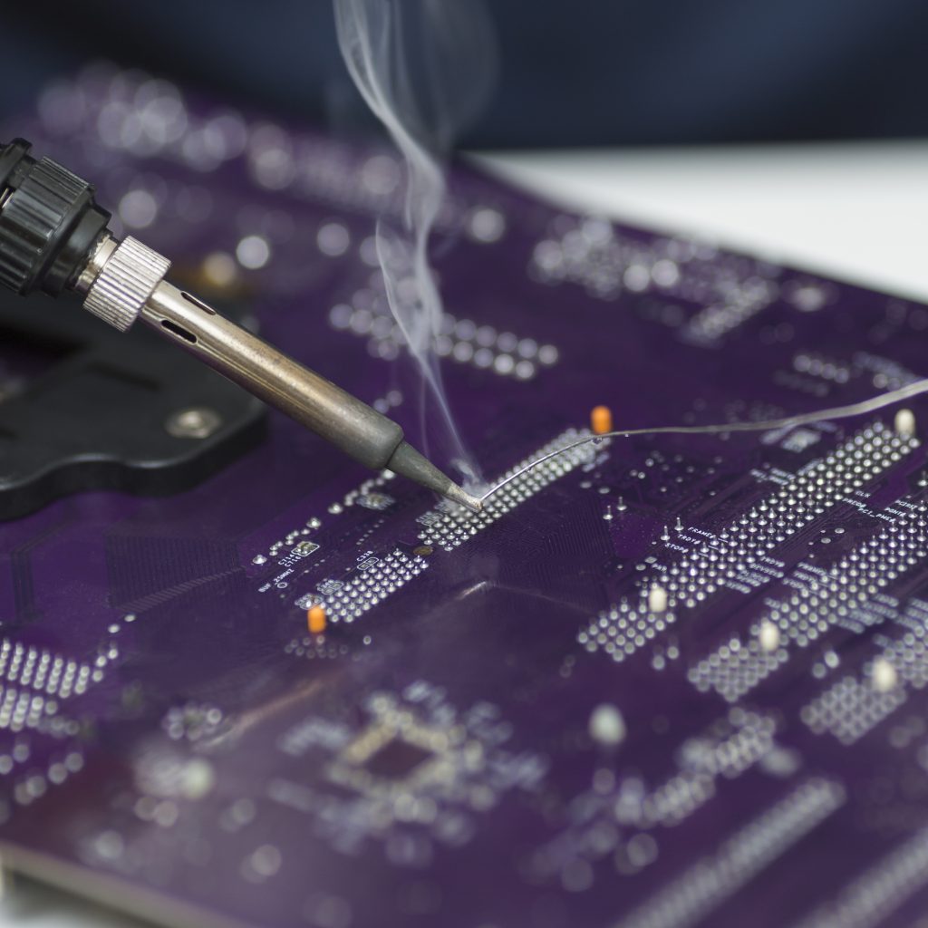
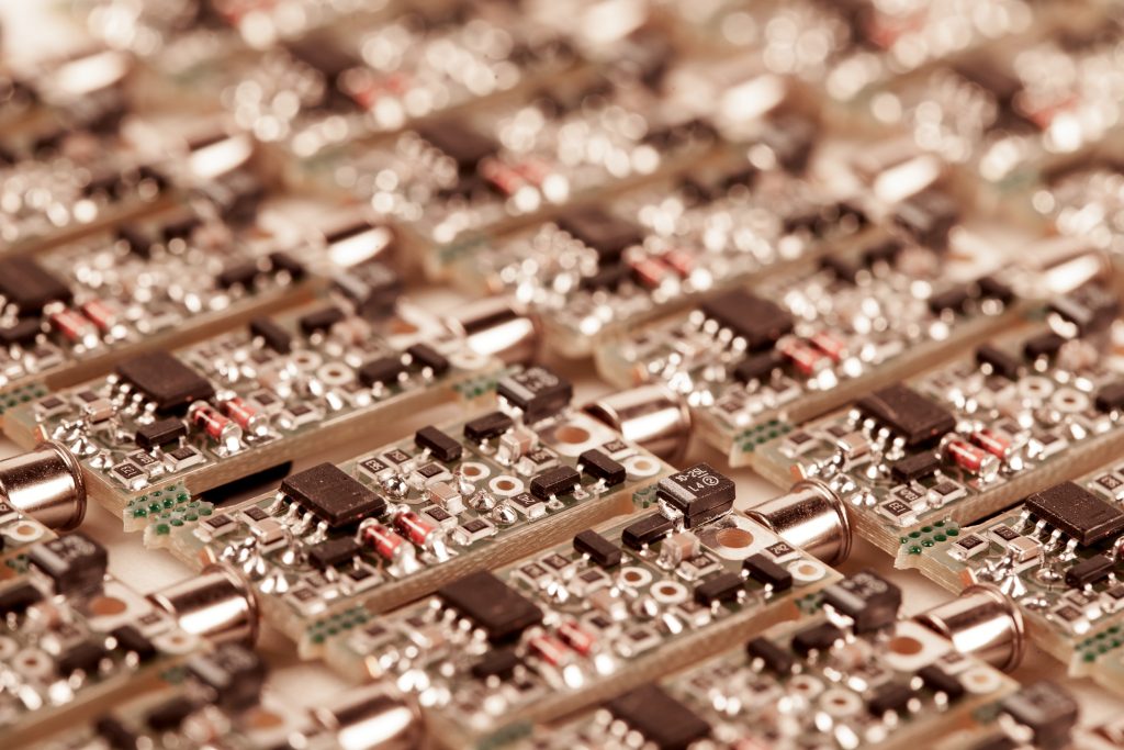
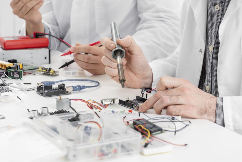
You can find a PCB assembly within the equipment that has arisen with technology’s evolution, and their production is complicated. A PCB assembly company forms them, and various staff, such as engineers, must manufacture them properly.
But what is a PCB assembly? How is it different from a printed circuit board?
This blog discusses PCB assembly and the steps required to complete this procedure.
What is a PCB Assembly?
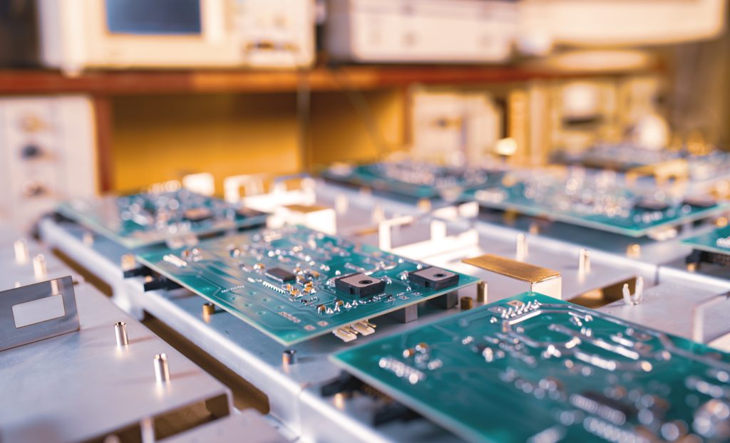
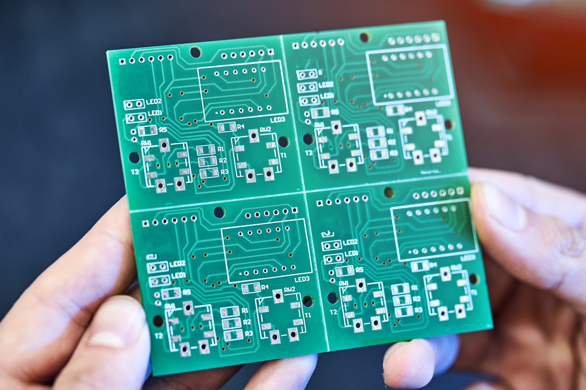
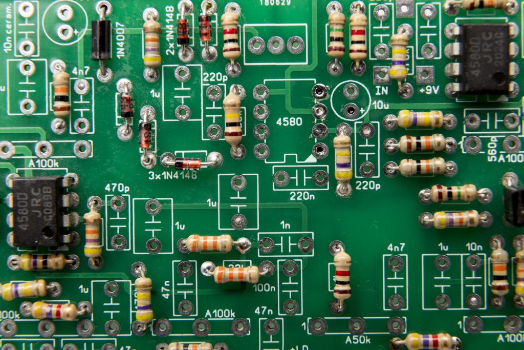
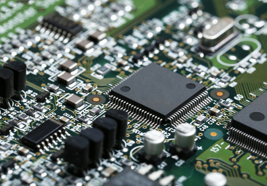
A printed circuit board assembly (PCBA) is a PCB with the electrical components soldered on. The circuit board is complete at this point.
A non-conductive substrate holds laminated copper sheets. The manufacturers engrave conductive pathways within these sheets.
Before its manufacturing is complete, a PCB assembly is known as a printed circuit board.
What are the components of a PCB?
Substrate
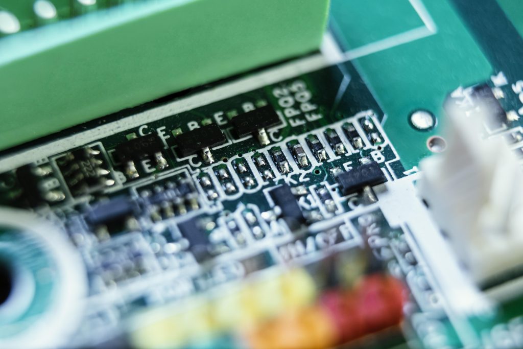
An FR-4 material (Fire Retardant – 4) forms the substrate and has a self-extinguishing property. The substrate is the rigid board to which professionals can solder different components.
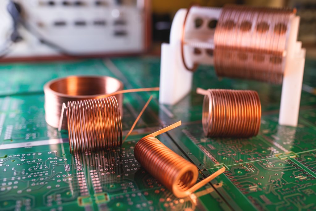
Copper Layer
Both the top and the bottom of the PCB have a layer of copper traces, which come from a thin copper foil.
Solder Mask
This layer is added to the top and bottom of the PCB to prevent short-circuiting. This protection is present as it separates the copper traces and acts as a non-conducive part of the PCB.
It also helps the solder go where it should, such as the pads and helps to avoid soldering onto other areas of the board.
Silkscreen
There is a silkscreen layer that contains essential information about the PCB. It acts as a reference for where components on the PCB should be and helps prevent errors when adding these components. Whilst the text and graphics are usually printed in white, other colours are available. The silkscreen layer is on top of the PCB.
How is a PCB manufactured?
1) PCB is designed
The PCB requires a design for creation. Various PCB assemblies are available, so the blueprint must meet the requirements for manufacturing a specific type. Designers often use the software Gerber X3 for this.
The design must be checked for errors twice, once after the software encodes the blueprint and then by a fabricator who completes the Design for Manufacture (DFM) check.
2) Design review and questions for engineers
An engineer then needs to check the design for errors or faults. They examine every part, and the process includes going through a design review. The engineer needs to approve the blueprint before printing.
3) PCB design printing
Printing a PCB design uses a plotter printer. The printer uses two colours for the inside layers of the PCB, clear ink to represent the non-conductive parts, such as the fibreglass base, and black ink for the copper traces and circuits.
For the outer layers, the black ink shows where there will be no copper, whereas the clear ink marks where the copper will be.
After printing, a punch machine inserts a registration hole into the relevant films, which is needed for film alignment later.
4) Copper is printed for interior layers
The manufacturers apply a layer of copper to the laminate material containing the printed PCB design. This layer can be a copper coating or a copper foil layer, and the laminate acts as the PCB’s structure.
The copper layer is pre-bonded to the laminate material before being etched away to show the blueprint.
Resist, a photo-sensitive film, is added to the laminate panel. When exposed to UV light, the photo-reactive chemical layer in the resist hardens, which enables the technicians to gain a perfect match in the photoresist with the blueprint photos.
The laminate and resist are lined up using the registration holes and exposed to UV light. The black ink blocks the light, so the resist beneath it doesn’t harden and can be removed later. The resist beneath the light film hardens so the copper can remain as pathways.
It is washed using an alkaline solution to remove the remaining photoresists, then pressure-washed and left to dry. Technicians check the PCB for any errors. After being popped out, the resist left should only be on the copper remaining on the PCB.
5) Etching the inner layers to remove copper
The more copper that needs removing, the longer this process can take. For example, larger PCBs can need more chemicals or a more extended timeframe for the etching to work.
Any additional copper in PCB’s inner layers needs to be removed. A covering protects the required copper, and adding a chemical to the board removes unnecessary metal.
Printed circuit board manufacturers need to perform additional steps to create multilayered PCBs. Many of them are the same as those required for single-layer PCBs, though each board layer needs these steps to take place. There is also usually copper foil between each layer instead of a copper coating.
The manufacturing of multilayered PCBs requires the following steps A-I. For single PCB assembly, the next step to follow is step 6, described later in this blog.
A) Inner layer imaging
Like the printing of the PCB design, inner layer imaging prints the blueprint from a plotter printer, creating a film. The printer also prints the solder mask for the inner layer. A resignation hole in the films helps line them up with other layers when appropriate.
Technicians add copper to the laminate and place the printed film over it. The registration holes align both layers. They are both exposed to UV light, where the resist beneath the light areas hardens, and the resist beneath the dark parts doesn’t.
B) Etching the inner layer
The hardened resist protects the necessary copper, whilst alkaline removes the soft resist. The unneeded copper is then exposed and removed using copper solvent via etching.
C) Resist stripping
The hardened resist protected the required copper, but it is now unnecessary. It would interfere with the copper’s conductive properties, so part of the PCB assembly process is to remove it. The PCB then needs to be inspected again.
D) Post-etch punch
The previously established registration holes are guides to line up the layers. A hole is then punched into them, using an optical punch guided by a computer, and checked. The alignment of the layers requires examining before proceeding to the next step.
E) Inner layer AOI (Automated Optical Inspection)
The inner layer of the PCB is inspected for remaining resist or incomplete patterns using a computer.
F) Inner layer oxide
The copper foil and insulating epoxy layers must bond between the inner and outer layers. Adding oxide to the inner layer enables this to occur better.
G) Layup
The insulating material and copper foil later bond between the inner and outer layers. Machines help with this process, which occurs when the layers are lined up and heated. They use machines because the layers and bonding must align precisely.
H) Lamination
When done correctly, a multilayer PCB contains effective insulation between the different layers, which are together tightly. Between the different layers is bonding epoxy. Pressure and heat during the lamination process melt this epoxy.
I) X-Ray Alignment
Holes must be drilled into the PCB to allow connections between the different layers. An X-ray ensures the drill is aligned correctly and that any holes drilled will be the right size and located in the correct place.
The next step in the multilayer PCB assembly process is step nine, which can be found later in the blog.
6) Aligning the layers
The outer and inner layers are aligned using the registration holes. An optical punch does this by inserting a pin through those holes, which aligns the layers.
7) AOI (Automated Optical Inspection)
After the layers are together, there is no way to alter any mistakes. The PCB, therefore, requires an inspection to ensure everything is correct. The automated optical inspection (AOI) machine compares the printed circuit board to the design in the software.
The technicians and the AOI machine check for errors to ensure there are no short circuits, extra copper present or any other issues.
8) PCB Layers are laminated
Fibreglass coated in epoxy resin form the outside of the PCB, and the original substrate piece holds a thin copper foil layer over the top. This copper foil contains copper trace etchings. The laminating process bonds these two layers together.
Pre-coated epoxy resin layers (also known as pre-impregnated), copper foil layers and substrate layers each fit with a specialised pin on a special press table in a specific order. A piece of copper called the press plate is on top.
A mechanical press pressures the layers, pushing them together and down. It also pushes the pins to fix the layers properly.
A laminating press melts the epoxy found within the pre-impregnated resin by applying heat and pressure to the layers using heated plates. A combination of the pressure and melted epoxy fuse the layers.
The manufacturer then accesses the PCB by removing the pins and top press plate.
9) Drilling and PCB plating
X-rays ensure that any drilling occurs in the correct places, and registration holes act as guidance to secure the PCB. The drill is computer-guided, using the design on Extended Gerber as a reference.
Filing removes additional copper found at the edges.
10) Outer layer imaging and etching
The outer layers of the PCB are coated in photoresist and imaged. After imaging, it also gets a tin plating to help protect the copper when the etching occurs.
In this situation, the tin protects the necessary copper whilst the copper solvent from earlier removes the excess. For the outer layer, the copper needing removal is covered by dark ink, whilst the clear areas cover the required copper.
Any resist that is still present is also removed at this stage.
11) Outer layer AOI
Another automated optical inspection takes place to identify any errors. It checks that the outer layer matches the design and that there is no excess copper to prevent improper electrical connections from occurring.
12) Solder mask application
The panels are cleaned and covered in ink epoxy and solder mask film. The UV light then hits the panels to show where the solder mask needs to remain and which parts need removing.
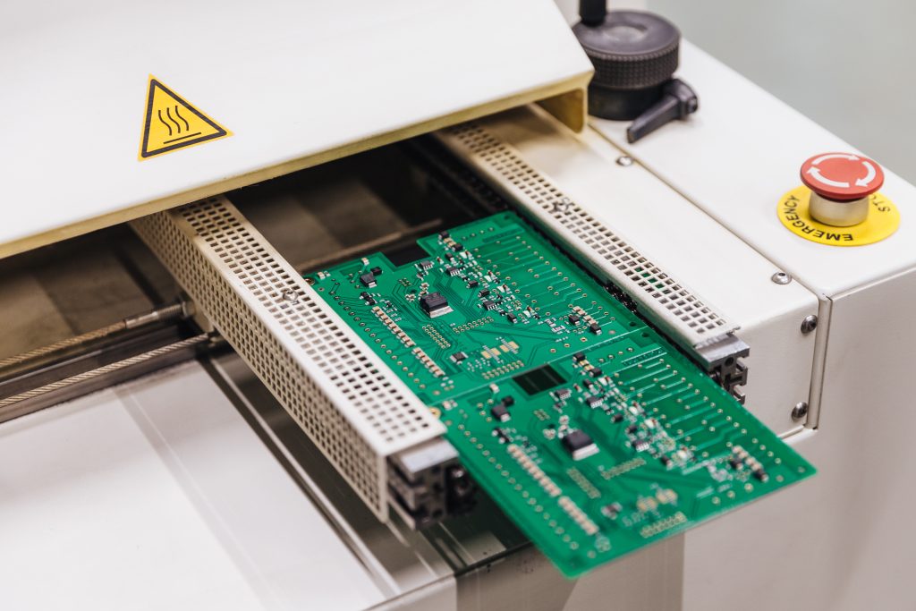
A technician removes the unneeded solder mask, and the PCB is put in an oven so the mask can cure to protect the copper from oxidation and corrosion damage.
13) Silkscreen and Surface Finish application
Silkscreen application is where essential data is printed on the board’s surface, usually using an inkjet printer. This information includes:
- Warning labels
- Pin locators and similar marks
- Part numbers
- Manufacturer marks or logos
- Company ID numbers
The PCB then has the surface finish added.
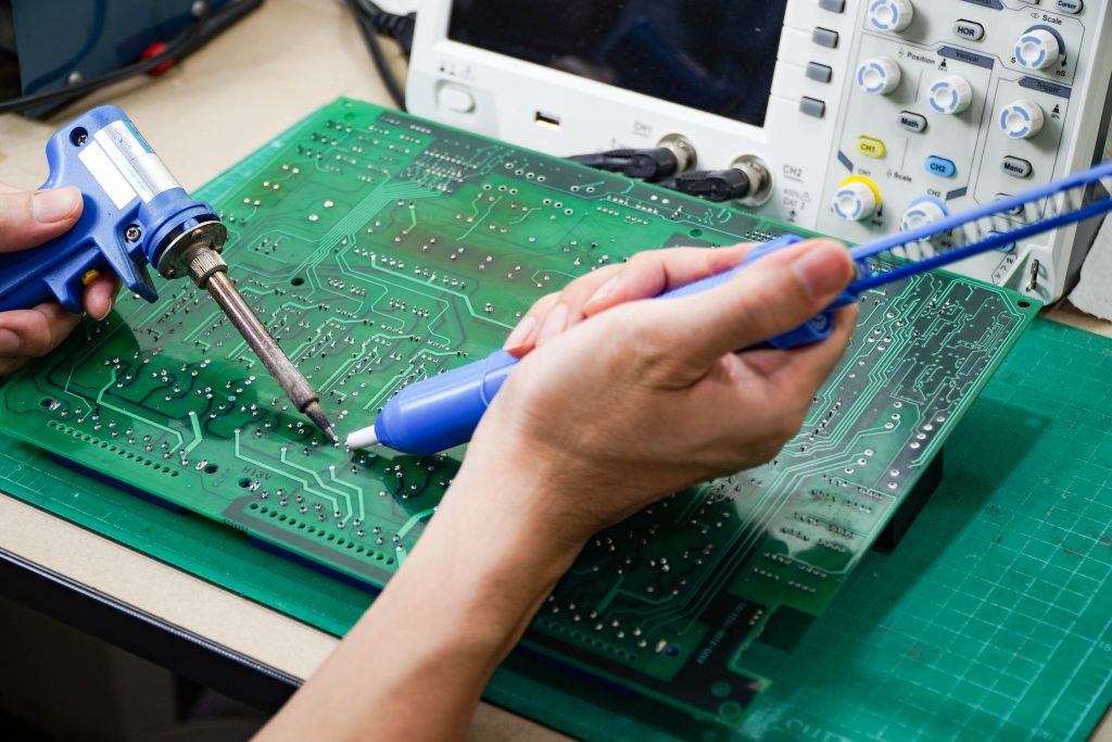
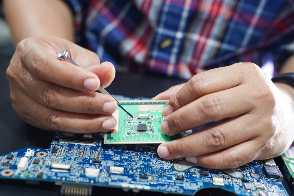
14) Finishing the PCB and subsequent electrical testing
The printed circuit board needs plating with conductive materials. The metal plating provides oxidation protection to the copper. The mounting of the electrical components can also now occur due to this plating.
Several different metals are available, including organic solderability preservative (OSP), immersion silver and lead-free HASL, though other options are available such as gold and nickel. Each metal has different properties, but the specific one needed will change depending on the customer’s budget and the design specifications.
The PCB then undergoes various tests, including electrical reliability testing. The electrical reliability testing includes isolation and circuit continuity tests, which check for shorts in the isolation valves and disconnections in the PCB, respectively.
The testing must meet the standards of IPC-9252, Guidelines and Requirements for Electrical Testing of Unpopulated Printed Boards.
The technician can also conduct other tests. These tests can include how the PCB responds to pressure.
15) Profiling
The fabrication engineers find the size and shape of each PCB cut from the construction board, which they can usually find within the Gerber files. This information impacts where they should make the scores on the board.
The scores allow the PCBs to separate easier without breaking. Often, a CNC machine adds small pieces along the board’s edges. Sometimes, a fabricator may add a v-groove instead, which is when the sides of the board contain v-shaped cuts.
The fabricators then break the boards from the construction board.
16) Quality check and compliance inspection
An additional check is needed to ensure everything is as it should be. For example, it identifies that the dimensions match the design specifications, the PCB has no sharp edges, and it has all passed the electrical reliability testing. They also look for hole sizes that must match the requirements and be the same in all the layers, and the boards must be clean and dust-free.
The PCB assembly process requires various steps, equipment and testing to ensure everything operates correctly, so you must find the best support and services for your situation.
Altimex can help you with your printed circuit boards, whether you need more information about the components or the process. Contact us today for more information about our services and see how we can help you with your PCB assembly needs.