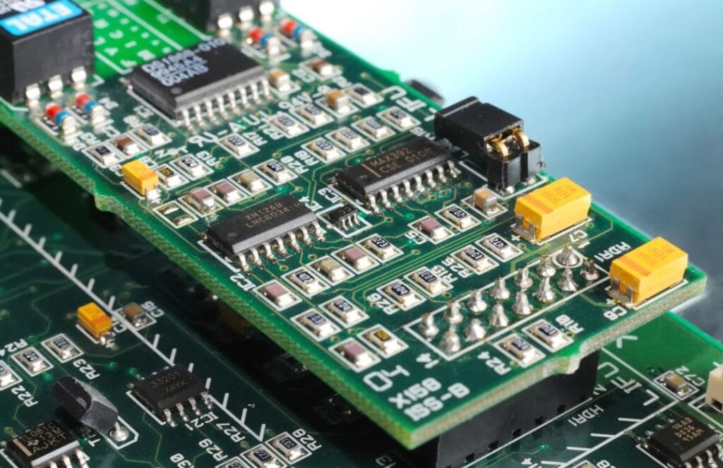
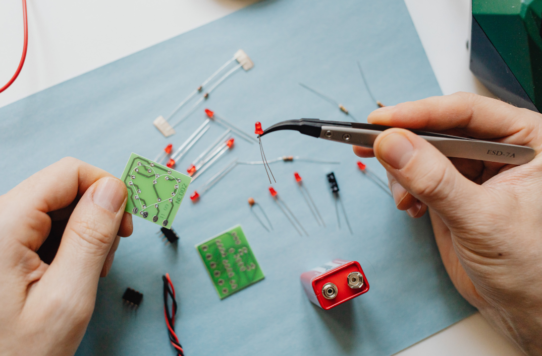
A PCB assembly drawing bridges design and production, helping engineers and manufacturers speak the same language. When drawings are incomplete, errors and costly delays soon follow.
To create a PCB assembly drawing, you simply translate your design data into clear circuit board assembly instructions that technicians can follow without guesswork.
Gathering Design Files and Component Data
Before starting any PCB drawing guide, collect every file that defines your circuit. Missing or outdated data can cause production delays, so staying organised is key to strong PCB documentation standards.
Your design pack should include:
- Gerber files for copper layers and silkscreen.
- Bill of Materials (BOM) listing components and quantities.
- CAD or pick-and-place files with coordinates and rotation.
- Drill and outline files for holes and board edges.
- Revision notes for version control.
This stage shapes the success of your electronics manufacturing documentation and sets up a smoother PCB assembly process later.
Defining the Purpose and Scope of the Drawing
A PCB assembly drawing turns complex design data into clear instructions for production teams. It shows exactly how each component should be placed and oriented, reducing the risk of costly mistakes.
Following assembly drawing best practices keeps communication consistent and avoids confusion between design and assembly teams. Prototype drawings might only show basic placement, whereas production versions include tolerance notes and manufacturing instructions.
This balance of detail and clarity supports better PCB design for manufacturing and ensures every build follows the same standard.
Setting Up Drawing Templates and Standards
Before adding components, set up a drawing template that follows recognised PCB documentation standards. Templates create structure and consistency, helping every engineer read the same information in the same way. Many teams follow IPC-D-325 or adapt their own company format.
Each drawing should include:
- Title block – project and company details.
- Revision field – date and designer.
- Board view references – top and bottom orientation.
- Notes area – for manufacturing comments.
- Approval field – for quality sign-off.
This framework keeps your electronics manufacturing documentation consistent and supports accuracy throughout the PCB assembly process.
Adding Component Placement Details

Once your template is ready, show exactly where each component belongs. This step forms the visual core of any PCB drawing guide, giving assembly teams a clear view before soldering begins.
Include every outline, reference designator, and polarity mark so placement is unambiguous. Show top and bottom views separately and use colour-coded layers in your CAD tool for readability. These details make complex layouts easier to interpret and reduce production confusion. Clear placement drawings also strengthen the PCB assembly process, improving communication and accuracy from the start.
Including Reference Designators and Labels
Clear labelling is one of those details that might seem minor yet often decides whether an assembly run goes smoothly or not. Reference designators act as the link between your PCB assembly drawing, the Bill of Materials, and the actual board. When these markers are inconsistent, technicians can lose time cross-checking or, worse, place components incorrectly.
Consistency, as simple as it sounds, is central to assembly drawing best practices. Every reference designator should match the BOM exactly, same case, same spelling, same position. Adding these labels in a logical, readable order (usually left-to-right or top-to-bottom) helps speed up verification later.
Here’s a short checklist to follow:
- Use clear, legible font sizes visible after printing.
- Keep designators outside the component outline, never overlapping pads.
- Mirror labels for bottom-layer views to prevent confusion.
- Double-check alignment with the BOM and pick-and-place data.
- Update designators promptly when components move during revision.
Following this simple list might sound routine, yet it’s a small step that often prevents the biggest mistakes during the PCB assembly process.
Highlighting Polarities and Orientation Marks
Orientation errors can halt production, so your PCB assembly drawing must clearly show polarity and direction. A reversed diode or rotated IC can cost hours to fix, which is why these indicators are essential. Use consistent symbols that match your CAD data and stand out on the print.
Common notations include:
- Diodes: stripe or triangle for the cathode.
- Capacitors: plus or minus sign for polarity.
- ICs: dot or notch marking pin one.
- LEDs: arrow direction for current flow.
These small cues might seem simple, yet they’re key to any PCB drawing guide and prevent costly rework during the PCB assembly process.
Specifying Notes and Manufacturing Instructions
The notes section of your PCB assembly drawing might not look exciting, yet it often carries the details that keep production consistent. These written instructions tell the manufacturer exactly how the board should be handled, soldered, and inspected, all crucial parts of good PCB design for manufacturing practice.
It’s best to keep notes brief and standardised, using clear language instead of vague technical phrases. Overly long paragraphs can lead to misinterpretation, whereas short, direct points reduce the risk of confusion. Most engineers prefer to group instructions under clear headings such as “Assembly,” “Soldering,” and “Inspection.”
| Example Notes | Recommended Alternatives |
| Apply solder as needed | Use no-clean flux solder as specified |
| Check alignment before soldering | Verify component orientation before final soldering |
| Clean board if necessary | Clean only if visible residue remains |
Keeping these details accurate is a small but meaningful way to maintain strong electronics manufacturing documentation. They help every operator understand your intent without back-and-forth clarification, leading to a smoother PCB assembly process overall.
Reviewing and Verifying for Accuracy
Before sending your PCB assembly drawing to production, take a moment to double-check every element. Verification tends to be the quiet step that saves the most time later, especially when several teams handle the same files. A short, methodical review can prevent expensive rework and make the PCB documentation standards you’ve set truly worthwhile.
Here’s a practical checklist to follow before submission:
- Confirm all component alignments match the CAD layout.
- Review layer visibility for top, bottom, and internal sections.
- Check annotation clarity; every designator and note should print cleanly.
- Cross-reference BOM and netlist data for consistency.
- Verify orientation and polarity marks against component datasheets.
Once these checks are complete, it’s always a good idea to ask a colleague or your manufacturer to review the drawing as well. Peer feedback usually spots small errors you might miss.
In the meantime, if you’d like professional input or help refining your documentation, feel free to contact us; our team here at Altimex are happy to review your design package and help strengthen your next PCB assembly process.


