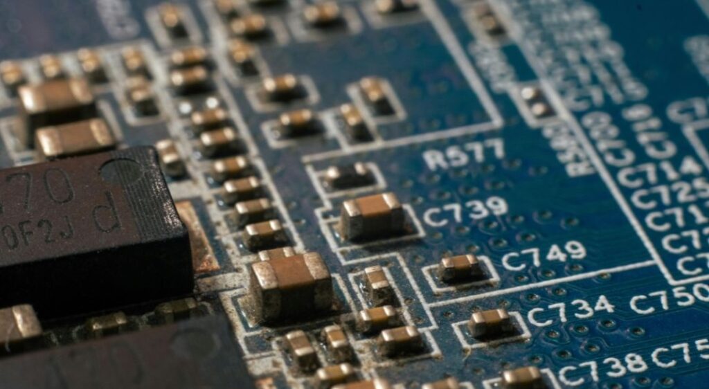
Modern printed circuit boards rely on dependable electrical interconnections between copper layers. In multilayer designs, signals and power must transfer between internal planes without compromising mechanical stability or long-term reliability.
Within this structure, plated through-holes (PTH) act as conductive pathways. A plated through-hole is a drilled opening in a PCB that has been lined with copper. The copper forms a continuous barrel connecting one layer of the board to another, creating stable PCB electrical connections throughout the stack.
When used for component mounting, through-hole components pass through these plated openings and are soldered to pads on the surface. The plated barrel provides electrical continuity between layers, and the solder joint delivers mechanical anchoring.
This approach forms a core element of through-hole PCB technology and remains a fundamental part of the PCB manufacturing process. It has supported electronics production for decades and continues to be specified where durability, current capacity and multilayer PCB connectivity are design priorities.
How Plated Through-Hole Technology Works
In PCB fabrication, plated through-holes are formed through a controlled sequence of mechanical and chemical processes. Each stage influences the electrical performance and structural integrity of the finished board.
The process typically includes:
Drilling through the PCB stack
CNC drilling machines create holes at defined coordinates through the laminated board. Accuracy is measured against design tolerances and annular ring requirements to prevent breakout or misalignment.
Desmear and hole wall preparation
Drilling leaves resin smear and debris on the internal surfaces. Chemical treatment removes contamination and exposes clean copper on inner layers. This stage determines how effectively plating bonds to both substrate and copper.
Electroless copper deposition
A thin conductive seed layer is deposited on the non-conductive hole wall. This enables subsequent electroplating.
Electrolytic copper plating
Copper thickness is increased inside the hole using electroplating. IPC-6012 performance classes define minimum plating thickness requirements. Insufficient barrel thickness increases the risk of cracking under thermal cycling.
Formation of the conductive barrel
The plated copper creates a continuous sleeve linking connected layers across the PCB.
Component insertion and soldering
Where holes are used for through-hole components, leads are inserted and soldered. The solder forms a metallurgical bond between the component lead and the plated barrel, completing the electrical path.
Controlled drilling parameters, plating chemistry management and inspection processes determine the reliability of plated through hole PCBs in production. At Altimex, structured process control and inspection frameworks support consistent interlayer connectivity across batches.
Scale Your Production
From prototype to full-scale electronic assembly, our UK facility is equipped to handle your requirements.
Get a QuoteKey Benefits of Plated Through-Hole PCBs
Plated through-holes remain widely specified in PCB design where mechanical and electrical reliability are central concerns.
Key advantages include:
- Mechanical strength
Component leads secured within plated barrels resist vibration and mechanical load more effectively than surface-only attachment. - Thermal endurance
The copper barrel distributes heat along its length. Adequate plating thickness reduces fatigue during repeated temperature cycling. - Higher current handling
Through-hole components often use larger leads and pads, supporting connectors, transformers and power devices with elevated current demand. - Reliable multilayer interconnection
Plated barrels create stable electrical links between internal copper layers in complex stack-ups. - Serviceability
Through-hole components are often easier to replace during prototyping or maintenance.
These properties make through-hole PCB technology relevant in systems where electrical continuity and physical durability carry operational consequences.
Plated Through-Hole PCB vs Surface Mount Technology
Through-hole and surface mount assemblies represent different approaches within PCB design. Many modern boards combine both methods.
| Feature | Through-Hole Technology | Surface Mount Technology |
| Mounting method | Leads pass through plated holes | Components attach directly to surface pads |
| Mechanical retention | Strong anchoring through barrel and solder | Lower structural retention |
| Current capacity | Suitable for higher current devices | Typically lower current handling |
| Board density | Requires more space | Enables higher component density |
| Assembly speed | Slower insertion processes | High-speed automated placement |
| Rework | Often simpler to replace components | Fine-pitch parts can be harder to rework |
| Typical use | Power stages, connectors, industrial hardware | Consumer electronics, compact designs |
In practice, engineers often select surface mount for signal circuitry and retain plated through-holes for mechanically stressed or high-current components.
Engineering-Led Solutions
Work with a team that understands modern electronics and end-to-end manufacturing.
Our ExpertiseCommon Applications of Plated Through-Hole PCBs
Plated through-holes remain present in industries where reliability margins must be maintained over long service intervals.
Aerospace and defence electronics
Exposure to vibration and thermal variation demands secure component retention.
Industrial machinery
Control systems and power electronics experience mechanical stress and electrical load cycling.
Telecommunications infrastructure
Network equipment requires stable PCB electrical connections across extended operating life.
Automotive electronics
Vehicle control modules operate under vibration and temperature fluctuation.
Medical devices
Certain systems depend on consistent electrical performance across regulated environments.
Power supplies and high-current systems
Transformers, large connectors and power devices rely on through-hole mounting for mechanical support and conductivity.
Types of Plated Through Holes in PCBs
Different plated hole structures perform distinct functions within multilayer PCBs.
Vias
Small plated holes transferring signals between layers.
Through vias
Extend from top to bottom, connecting the full board thickness.
Blind vias
Link an outer layer to one or more inner layers without passing completely through.
Buried vias
Connect internal layers only and remain enclosed within the board.
Component mounting holes
Larger plated openings supporting through-hole components.
Each structure supports PCB electrical connections across defined layers within the stack.
Ready to start your project?
Contact our technical team today to see how Altimex can streamline your electronics supply chain.
Contact UsManufacturing Considerations for Plated Through-Hole PCBs
Designers must account for fabrication constraints early in development.
Key engineering considerations include:
- Hole aspect ratio
The ratio between board thickness and hole diameter affects plating uniformity. High aspect ratios increase the risk of uneven deposition. - Copper barrel thickness
Meeting IPC performance class requirements reduces the likelihood of fatigue cracking under thermal stress. - Annular ring dimensions
Adequate pad width prevents breakout and supports solder joint reliability. - Thermal stress during soldering
Expansion mismatch between copper and substrate material can influence barrel integrity. - Inspection and verification
Electrical testing, automated optical inspection and microsection analysis confirm plating thickness and hole wall quality.
Early design collaboration with the manufacturer reduces avoidable revisions at production stage. Altimex supports customers through design review and manufacturing validation aligned with defined quality standards.
Challenges and Limitations of Plated Through-Hole Technology
Through-hole PCB technology presents constraints in dense electronic designs.
Limitations include:
- Larger component footprint
- Reduced routing area due to drilled holes
- Slower automated assembly
- Potential cost increase in high-density layouts
- Reduced suitability for ultra-compact devices
Design teams balance these factors against mechanical and electrical reliability targets.
The Future of Plated Through-Hole PCBs
Plated through-holes continue to operate alongside surface mount methods in hybrid PCB assemblies.
Advances in drilling precision, plating chemistry control and inspection methods support continued use in industrial control, automotive electronics and power systems. Through-hole PCB technology remains relevant where structural anchoring and current handling are non-negotiable design requirements.
Frequently Asked Questions About Plated Through-Hole PCBs
What is the difference between plated and non-plated holes?
Plated holes contain conductive copper lining the hole wall. Non-plated holes provide mechanical fixing without electrical interconnection.
Are plated through hole PCBs still used today?
Yes. Many industrial and power-focused systems rely on plated through-holes for structural stability and electrical continuity.
When should engineers choose through-hole components?
When higher current capacity, stronger mechanical retention or reinforced multilayer PCB connectivity is required.
Are through-hole PCBs more durable than SMT boards?
Through-hole connections often provide stronger mechanical anchoring under vibration or load.
What industries rely on plated through-hole technology?
Aerospace, industrial control, telecommunications infrastructure, automotive systems and power electronics.
For technical guidance on PCB manufacturing or product design support, contact us to speak with the Altimex engineering team.