

Design for Manufacture (DFM)
Altimex provides PCB design for manufacture services for UK businesses preparing electronic products for production. Our engineers review PCB layouts, component placement, materials, panelisation and assembly requirements to identify potential manufacturing issues before work begins. By reviewing each design early, Altimex can reduce delays, avoid unnecessary rework and support PCB assembly. All recommendations are based on industry standards, including IPC-A-610 and IPC-J-STD-001.
✓ Prototype to Volume Production
✓ UK-Based PCB Manufacturing
✓ Quality-Assured PCB Solutions





What Is PCB Design for Manufacture?
PCB design for manufacture is the process of reviewing a PCB design before production to identify issues that could affect assembly, testing, quality or cost. This can include checks on component placement, pad sizes, spacing, materials, panelisation and manufacturing tolerances.
Altimex has more than 30 years of experience in PCB assembly and electronic manufacturing. From its Cheshire facility, the team supports businesses across aerospace, automotive, telecommunications, defence and maritime, helping prepare PCB designs for efficient production and consistent assembly quality.
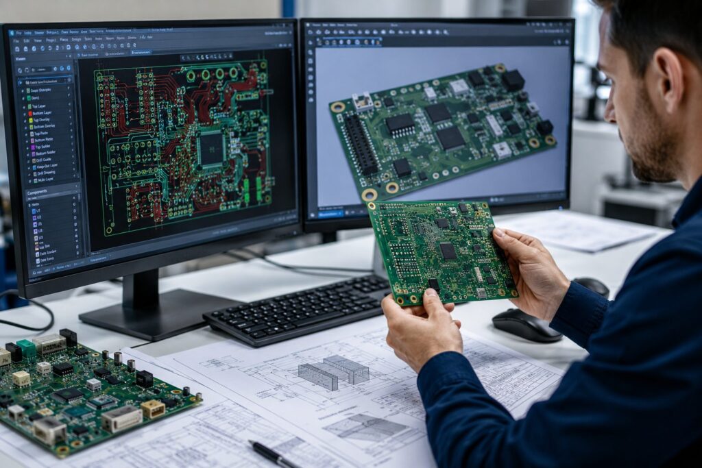
Our Mixed Technology PCB Assembly Capabilities
Altimex combines surface mount and through-hole assembly processes to manufacture PCB assemblies containing a wide range of component types. Each stage is planned around the board layout, component requirements and expected production volume, supporting accurate assembly from prototypes through to repeat production.
Altimex uses automated surface mount assembly equipment for the accurate placement of compact and fine-pitch components. Controlled solder paste application, component placement and reflow soldering support consistent results across prototypes, low-volume batches and repeat production.
Through-hole components are inserted and soldered using controlled manual or automated processes. This method is suited to connectors, transformers, larger components and parts that require strong mechanical connections or additional support.
Surface mount and through-hole components are assembled on the same PCB using a planned production sequence. Our engineers review component placement, soldering requirements and thermal considerations to reduce manufacturing risks and maintain consistent assembly quality.
Mixed technology PCB assemblies are inspected throughout production using visual checks, automated inspection and testing options based on the project requirements. Work is completed in line with IPC-A-610 and IPC-J-STD-001 standards.
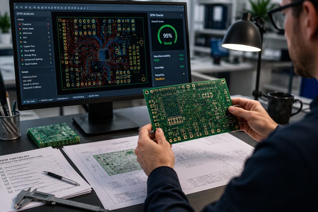
Component Review for PCB Design for Manufacture
Altimex reviews component choices as part of the PCB design for manufacture process. Our engineers check footprints, package sizes, availability, lifecycle status and suitability for the planned assembly method, helping identify risks before production begins.
The bill of materials is reviewed for obsolete parts, long lead times and possible alternatives. Any suggested changes are shared for approval, helping reduce delays, prevent placement issues and support consistent assembly quality.
Altimex provides PCB design for manufacture services to identify layout, component and production issues before assembly begins. Our engineers review PCB data, bills of materials, component footprints, panelisation and testing requirements.
We support prototype, low-volume and repeat production projects. Contact Altimex to discuss your PCB design, manufacturing requirements and project timescales.
Why Work With Altimex?

30+ Years Of Experience

Fast Turnaround Time

Tailored
Solutions

Building Long-Term Partnerships

Certified & Experienced Team
Our PCB Design for Manufacture Process
Altimex follows a structured PCB design for manufacture process to identify issues before production begins. Each project is reviewed by experienced engineers, with checks based on the board layout, component selection, assembly method, testing needs and production quantities.
- PCB design and manufacturing review
- Bill of materials review
- Component footprint and placement checks
- Pad, spacing and clearance review
- Panelisation and tooling review
- Assembly and soldering assessment
- Inspection and testing review
- Manufacturing feedback and recommendations
- Final design approval before production
Sectors we support.
Electronics manufacturing for applications where quality, reliability and consistent performance matter.




What Is PCB Design for Manufacture Used For?
PCB design for manufacture is used to identify potential production issues before a board moves into assembly. It helps check component placement, footprints, spacing, panelisation, soldering access and testing requirements, reducing the risk of delays, rework and inconsistent build quality. Altimex supports DFM reviews for prototype, low-volume and repeat production projects across industrial, automotive, aerospace, communications, medical and defence applications.
Frequently Asked Questions
What is PCB design for manufacture?
PCB design for manufacture is the review of a printed circuit board design before production begins. It checks whether the board can be assembled, soldered, inspected and tested efficiently using the planned manufacturing process.
Why is a DFM review needed before PCB assembly?
A DFM review can identify layout, spacing, footprint, component and panelisation issues before they cause production delays or assembly faults. Addressing these concerns early can reduce rework, wasted materials and unexpected manufacturing costs.
What does Altimex check during a PCB DFM review?
Altimex can review component placement, pad sizes, footprints, clearances, board dimensions, panelisation, tooling areas and test access. The review is based on the PCB data, bill of materials and intended assembly method.
Can DFM identify component footprint issues?
Yes. Component footprints can be checked against package dimensions, pad layouts and placement requirements. This helps identify incorrect or unsuitable footprints that may cause soldering, placement or inspection problems during production.
Does PCB design for manufacture include a bill of materials review?
Yes. The bill of materials can be reviewed for component availability, lifecycle status, package compatibility and possible supply risks. Obsolete parts, long lead times or suitable alternatives can be raised before assembly begins.
Is DFM suitable for prototype PCB projects?
Yes. DFM is useful for prototype projects as it can identify production concerns before the first boards are assembled. The findings may help engineers refine the design before approving low-volume or repeat production.
Can Altimex review panelisation requirements?
Yes. Altimex can review panel layouts, tooling areas, fiducial marks, board spacing and separation methods. Suitable panelisation can improve handling, automated placement and consistency during PCB assembly.
What files are needed for a PCB DFM review?
Common files include Gerber data, drill files, a bill of materials, placement data and assembly drawings. Further specifications may be requested depending on the board design, component types and testing requirements.
Which industries use PCB design for manufacture services?
PCB DFM services are used across industrial, medical, automotive, aerospace, communications, defence and maritime electronics. They are suitable for projects where reliable assembly, consistent quality and controlled production are required.