

When components arrive at a PCB assembly facility, the manufacturing process is only just beginning. Reliable PCB assembly depends on a series of controlled procedures designed to verify materials, maintain traceability, support production efficiency and reduce quality risks before a board ever enters an assembly line.
Many organisations focus on the finished product, yet the preparation stages that take place after component delivery can have a significant influence on assembly quality, production consistency and long-term reliability. Incorrect parts, poor storage conditions, missing documentation or inadequate verification can create issues that become far more costly to resolve later in the process.
Professional PCB assembly providers use structured workflows to ensure every component, circuit board, and production requirement is validated before assembly begins. These controls help support reliable outcomes while providing greater transparency throughout manufacturing.
Understanding what happens after PCB components arrive can help procurement teams, OEMs and product developers assess what good PCB assembly practice looks like and what questions to ask when evaluating a manufacturing partner.
Incoming Component Inspection
Incoming inspection helps manufacturers identify damaged, incorrect or inconsistent components before production begins.
The first stage after component delivery involves checking materials against purchase orders, delivery documentation and production requirements. The objective is to confirm that everything required for assembly has arrived in suitable condition.
Packaging is inspected for signs of physical damage that may have occurred during transit. Component reels, trays and moisture-sensitive packaging are examined to ensure protective materials remain intact.
Quantity verification is also important. Missing parts can disrupt production schedules, while surplus deliveries may create inventory management challenges if they are not identified early.
Supplier information is reviewed to confirm that components originate from approved sources and match production requirements. This process supports quality control while helping reduce the risk of incorrect or unauthorised parts entering the assembly workflow.
A common example involves discovering an incorrect component reel during incoming inspection. Identifying the issue before production begins allows corrective action to take place without disrupting assembly operations or creating rework further down the line.
Early stage inspection acts as a safeguard for the entire manufacturing process. Problems identified at this stage are significantly easier to manage than defects discovered after assembly has begun.
Scale Your Production
From prototype to full-scale electronic assembly, our UK facility is equipped to handle your requirements.
Get a QuoteComponent Verification and Quality Checks
Component verification ensures the correct parts, specifications and revisions are used during PCB assembly.
Receiving the right quantity of components does not automatically guarantee manufacturing readiness. Every part must also be verified against the bill of materials (BOM), assembly documentation and product revision requirements.
Verification procedures typically include:
- Part number validation
- BOM matching
- Revision confirmation
- Specification checks
- Tolerance verification
- Supplier documentation review
These checks help ensure assembly teams are working with the intended components throughout production.
Revision control is particularly important. A component may appear identical to a previous version while containing specification differences that affect performance, compatibility or regulatory compliance.
For example, a revised component may introduce electrical characteristics that differ from those used during product validation. Discovering the discrepancy during verification prevents assembly delays and avoids unnecessary troubleshooting later.
This stage also supports counterfeit prevention measures. Reviewing supplier documentation and component markings helps manufacturers identify potential concerns before production begins.
A structured verification process forms a key part of any professional PCB assembly process because assembly accuracy depends on using the correct components from the outset.
Storage Conditions for PCB Components
Proper storage conditions help protect PCB components from moisture, contamination and environmental damage before assembly.
Electronic components can be sensitive to environmental conditions long before they are placed onto a circuit board. Effective storage procedures help preserve component integrity and maintain assembly quality.
Humidity control is particularly important for moisture-sensitive devices. Excess moisture absorbed during storage can affect assembly performance when components are exposed to soldering temperatures.
Temperature stability also plays an important role. Excessive environmental fluctuations can affect packaging materials, storage life and component condition.
Electrostatic discharge (ESD) protection forms another critical consideration. Many electronic components can be damaged by static electricity, even when no visible signs of damage are present. Controlled handling procedures help reduce this risk throughout storage and preparation activities.
Shelf-life management is equally important. Certain materials, including solder-related consumables and specialist components, may have defined storage limitations that require careful monitoring.
A practical example involves components stored outside recommended environmental conditions. Even if the parts appear visually acceptable, solderability issues may emerge during assembly, creating avoidable production complications.
Storage controls may seem routine, yet they contribute directly to manufacturing consistency and long-term product reliability.
Engineering-Led Solutions
Work with a team that understands modern electronics and end-to-end manufacturing.
Our ExpertisePCB Kit Preparation Before Assembly
PCB kit preparation organises components, boards and manufacturing documentation before production begins.
Before assembly can start, materials must be organised into complete production kits containing everything required for the scheduled build.
This process typically involves:
- Gathering all required components
- Confirming PCB availability
- Reviewing manufacturing documentation
- Checking assembly instructions
- Verifying production quantities
- Preparing materials for scheduled assembly
The objective is to ensure production teams have immediate access to everything required for efficient assembly.
Missing components discovered during production preparation can delay manufacturing schedules and disrupt workflow planning. Identifying shortages before assembly begins allows procurement teams and manufacturers to address issues proactively.
Documentation review also forms a key part of preparation. Assembly drawings, BOMs, revision information and manufacturing instructions must align before production progresses.
Effective preparation supports efficient PCB assembly operations by reducing avoidable interruptions once production starts.
While kit preparation receives little attention outside manufacturing environments, it plays an important role in maintaining workflow efficiency and production consistency.
Production Planning for PCB Assemblies
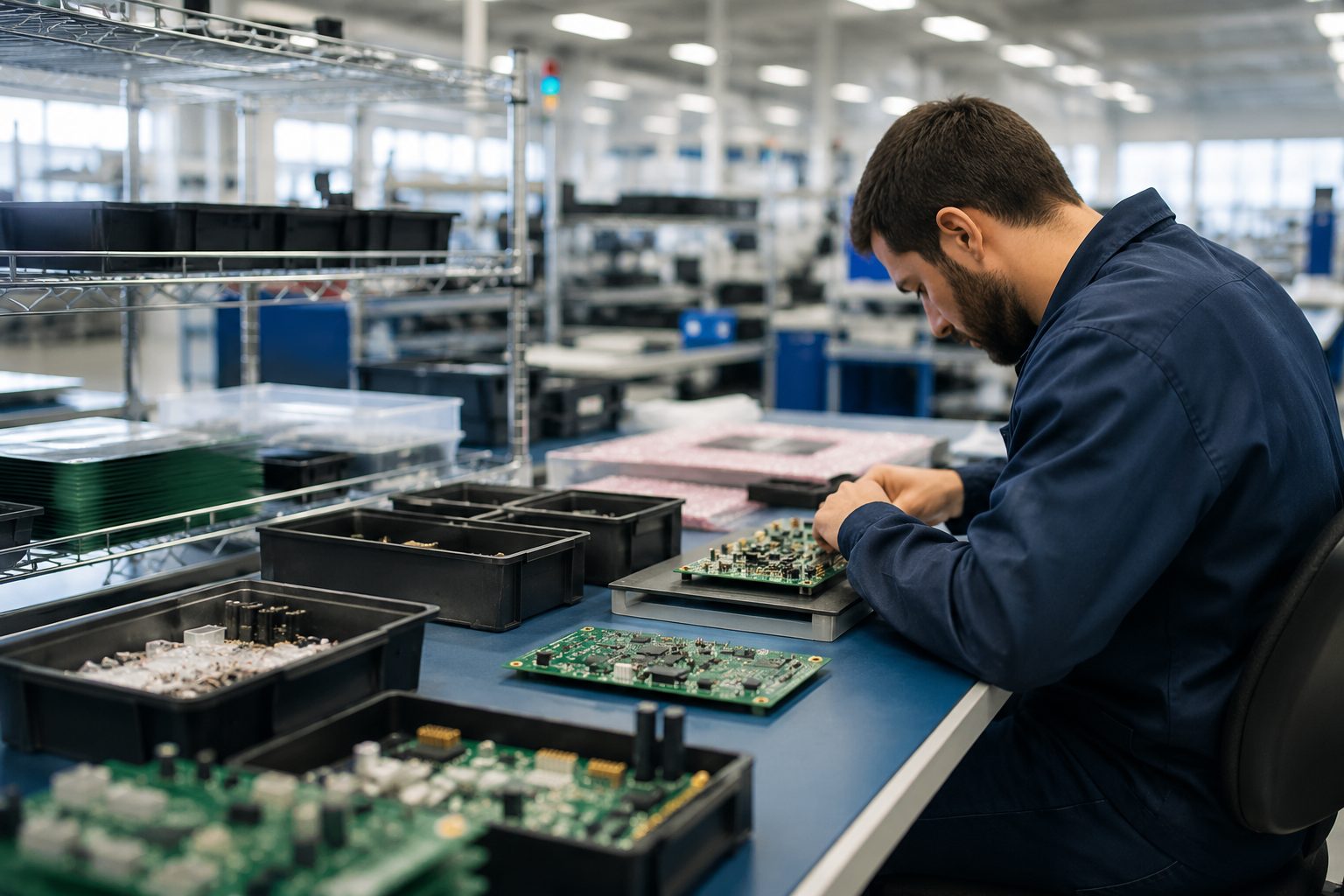
Production planning helps manufacturers coordinate materials, machine availability and assembly schedules efficiently.
Successful PCB assembly relies on more than component readiness. Manufacturing resources must also be coordinated effectively to support production requirements.
Production planning involves balancing:
- Assembly schedules
- Material availability
- Machine capacity
- Staffing requirements
- Quality control activities
- Delivery commitments
This coordination helps manufacturers allocate resources efficiently while maintaining production flow.
Scheduling becomes particularly important when multiple projects are progressing through the facility simultaneously. Priorities may need adjustment to accommodate urgent production requirements, engineering changes or customer delivery needs.
For example, an urgent production order may require assembly schedules to be reorganised while maintaining commitments across other active projects. Effective planning helps manage these situations without creating unnecessary disruption.
Production planning also supports machine setup efficiency. Grouping similar production activities can reduce changeover requirements and improve workflow continuity.
From a customer perspective, strong planning processes contribute to more predictable manufacturing outcomes and greater confidence in delivery schedules.
Ready to start your project?
Contact our technical team today to see how Altimex can streamline your electronics supply chain.
Contact UsTraceability Throughout PCB Assembly
Traceability systems help manufacturers track materials, assembly stages and quality records throughout PCB production.
Traceability provides visibility into how products move through the manufacturing process. It creates a documented record linking materials, assembly activities and quality control information.
Depending on product requirements, traceability may include:
- Component batch tracking
- Supplier records
- Assembly history
- Serial numbers
- Inspection records
- Testing documentation
These records become particularly valuable when investigating quality concerns or supporting compliance requirements.
Consider a scenario where a supplier later identifies a fault in a specific component batch. Good traceability allows manufacturers to quickly identify exactly which PCB assemblies used that batch, rather than quarantining entire production runs.
This reduces investigation time, limits unnecessary disruption and helps customers make faster decisions during quality investigations or field-return analysis.
Traceability also supports continuous improvement efforts by providing visibility into manufacturing trends and process performance over time.
Rather than viewing traceability as an administrative exercise, it is more useful to see it as a practical risk-management tool that supports accountability and manufacturing transparency throughout the production lifecycle.
Pick and Place Machine Setup
Pick and place setup ensures components are positioned accurately and efficiently during automated PCB assembly.
Automated placement equipment is responsible for positioning electronic components onto prepared circuit boards before soldering.
Before production begins, machines must be configured to match the specific assembly requirements of the product being built.
Setup activities typically include:
- Feeder loading
- Component verification
- Placement programming
- Calibration checks
- Alignment validation
- Trial production runs
Accuracy during this stage is critical. Even minor setup errors can affect assembly quality across an entire production batch.
A feeder loaded with the wrong component, for example, could introduce placement issues that require extensive rework if not identified during setup validation.
Even small setup errors can create widespread issues. A feeder offset of fractions of a millimetre may cause component misalignment across an entire batch, particularly on fine-pitch or high-density boards. Catching these issues during setup validation is significantly easier than reworking hundreds of completed assemblies.
Machine preparation also helps ensure that placement accuracy remains consistent across production volumes. This consistency becomes increasingly important when working with high-density PCB designs and fine-pitch components.
The value of pick and place preparation lies not in the machinery itself, rather in the controls that help maintain assembly precision throughout production.
Solder Paste Application Processes
Accurate solder paste application is essential for creating reliable solder joints during PCB assembly.
Before components can be soldered to a circuit board, solder paste must be deposited onto designated connection points.
Stencil printing is the most common method used to achieve this. A stencil aligns with the PCB and allows controlled amounts of solder paste to be applied to specific locations.
Consistency is critical, as too little solder paste may create weak connections. Excessive deposition can increase the likelihood of solder bridging and other assembly defects.
Process controls focus on:
- Paste consistency
- Stencil alignment
- Deposition accuracy
- Print quality verification
- Environmental control
Inspection procedures help confirm that solder paste has been applied correctly before component placement begins.
A practical example involves excessive solder paste volume creating unintended connections between adjacent pads. Detecting the issue before reflow soldering prevents more complex corrective work later in the process.
Solder paste application may appear straightforward, yet it forms one of the foundations of reliable PCB assembly.
Reflow Soldering During PCB Assembly
Reflow soldering permanently bonds components to the PCB using controlled thermal profiles.
Once components have been placed onto the board, assemblies pass through a reflow oven where carefully controlled heating cycles melt the solder paste and create electrical connections.
The process typically progresses through several stages, including preheating, temperature ramping, solder reflow and controlled cooling.
Thermal profile management is essential because different components and board designs respond differently to heat exposure.
If temperatures are too low, solder joints may not form correctly. Excessive temperatures can place unnecessary stress on components and materials.
A poorly controlled thermal profile may create reliability concerns that are not immediately visible during inspection. These issues can emerge later during product operation.
Manufacturers therefore monitor reflow conditions closely to ensure solder joints are formed consistently across production runs.
The objective is not simply to complete soldering. It is to create durable electrical and mechanical connections capable of supporting long-term product performance.
Automated Optical Inspection After Assembly
Automated optical inspection helps manufacturers identify placement, soldering and assembly defects quickly after production.
Following soldering, assembled boards typically undergo automated optical inspection (AOI). These systems compare completed assemblies against expected design parameters and identify potential defects.
AOI can help detect:
- Missing components
- Incorrect placement
- Polarity errors
- Alignment issues
- Soldering defects
- Component orientation concerns
The value of AOI extends beyond speed. Inspection provides a consistent method for identifying issues that may be difficult to detect during manual reviews alone.
For example, an incorrectly orientated component may pass through earlier stages unnoticed. AOI systems can identify the discrepancy before assemblies progress further into production.
Inspection findings also provide useful process feedback. Repeated defect patterns may highlight opportunities for manufacturing improvements or setup refinements.
AOI supports quality control by identifying potential issues early, reducing the likelihood of defective assemblies progressing through the remainder of the workflow.
Functional Testing and Final Quality Control
Functional testing and final inspection help verify that completed PCB assemblies operate as expected before shipment.
The final stages of PCB assembly focus on confirming that products meet manufacturing and operational requirements.
Testing activities may include:
- Electrical verification
- Functional validation
- Connectivity checks
- Programming verification
- Visual inspection
- Packaging review
The scope of testing varies depending on product complexity and customer requirements.
Functional testing provides an important opportunity to identify issues that visual inspection alone may not reveal. An assembly may appear physically correct while containing an intermittent electrical fault that affects performance during operation.
Identifying such issues before dispatch helps prevent avoidable disruptions after products reach customers.
Final quality control activities also confirm that assemblies have been packaged appropriately and prepared for shipment according to project requirements.
Reliable PCB assembly depends on process discipline at every stage, from incoming inspection through to final testing.
If you want to better understand how strong PCB assembly workflows improve quality, traceability and production consistency, Altimex can help. Contact us to discuss your product requirements and suitable manufacturing processes.