

Modern PCB assemblies contain increasingly compact layouts, higher component densities and more concealed interconnections than ever before. As electronic products become more sophisticated, verifying assembly quality through visual inspection alone becomes significantly more challenging.
Many of the defects capable of affecting performance, reliability or product lifespan exist beneath component packages or within solder joints that cannot be viewed directly. This creates a challenge for manufacturers, OEMs and product developers who need confidence that assemblies meet both functional and reliability requirements.
X-ray inspection addresses this challenge by providing visibility into hidden areas of a PCB assembly. Rather than focusing solely on external appearance, manufacturers can examine concealed solder joints, internal connections and potential defects before products move further through production.
Within advanced electronics manufacturing, X-ray inspection forms part of a broader quality assurance strategy. Alongside process controls, testing procedures and inspection workflows, it helps manufacturers identify hidden issues, validate assembly quality and support long-term product reliability.
X-Ray Inspection in PCB Manufacturing
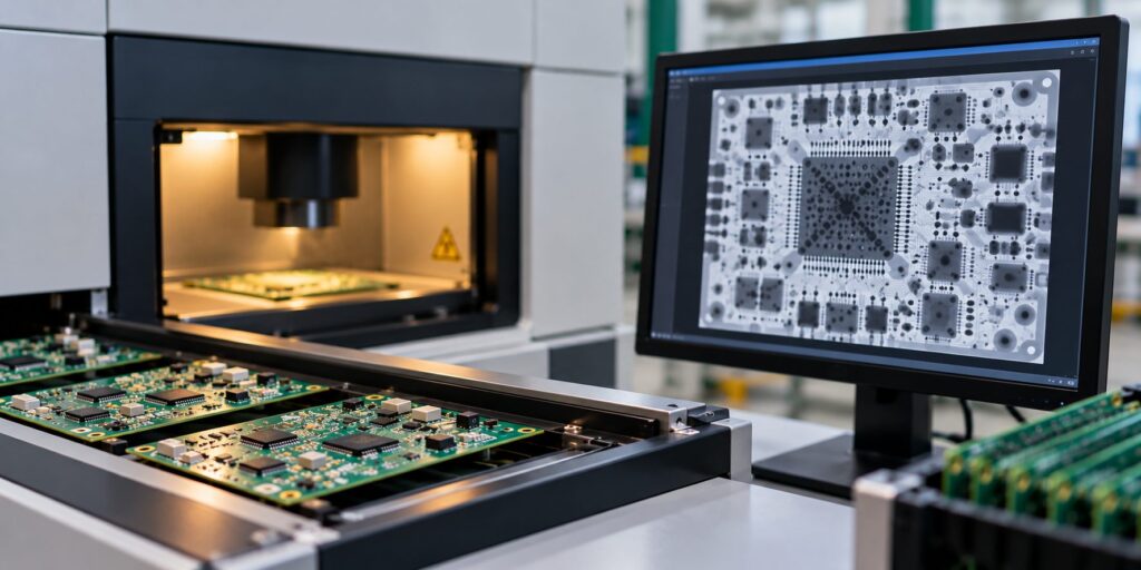
X-ray inspection allows manufacturers to examine hidden solder joints and internal PCB assembly features that cannot be inspected visually.
Unlike traditional visual inspection methods, X-ray systems provide visibility into areas concealed beneath components or within multilayer assemblies. This capability is particularly valuable as electronic products continue to become smaller and more densely populated.
Within a manufacturing environment, X-ray inspection is typically integrated into broader inspection workflows. Assemblies may pass through several quality checkpoints during production, with X-ray inspection used when hidden features require verification.
For example, a board containing ball grid array (BGA) components may appear acceptable from the surface. An X-ray image can reveal defects beneath the package that would otherwise remain undetected until functional testing or field deployment.
Understanding where X-ray inspection fits within the manufacturing process provides useful context when evaluating assembly quality requirements. Readers seeking a broader overview can explore Altimex’s guide covering everything you need to know about PCB assembly process.
The value of X-ray inspection lies not in the imaging technology itself, but in the visibility it provides into areas where hidden defects can develop.
Scale Your Production
From prototype to full-scale electronic assembly, our UK facility is equipped to handle your requirements.
Get a QuoteHidden Solder Joint Analysis
X-ray inspection helps identify hidden solder joint defects that cannot be detected through external visual inspection methods.
Many modern electronic components contain solder connections located beneath the package body. Once assembled, these connections become inaccessible to traditional inspection techniques.
Hidden solder joints can develop several types of manufacturing defects. These may include solder bridging, insufficient solder volume, incomplete wetting or internal void formation. While the external appearance of a component may seem acceptable, the underlying connection quality can vary significantly.
A practical example involves solder bridging beneath a concealed component. Two adjacent connections may unintentionally join during assembly, creating an electrical fault that remains invisible from the board surface. Without internal inspection, the issue may only become apparent during testing or after deployment.
Hidden defects matter because they can affect electrical performance, signal integrity and long-term reliability. Even when products initially function correctly, weak solder joints can become failure points when exposed to vibration, thermal cycling or extended operating conditions.
By identifying concealed issues during production, manufacturers gain greater confidence in assembly quality before products progress through later manufacturing stages.
BGA Inspection and Fault Detection
Ball grid array components require X-ray inspection because their solder joints are concealed beneath the component package.
BGAs are widely used within modern electronics because they support high connection counts while minimising board space requirements. Their compact design makes them highly effective for advanced assemblies, though it also creates inspection challenges.
Once a BGA has been soldered to a PCB, the solder balls become hidden between the component and the board surface. Visual inspection cannot assess the condition of these joints directly.
X-ray inspection allows manufacturers to evaluate solder integrity, alignment and connection quality beneath the package. Engineers can identify missing solder connections, misalignment issues, bridging defects and voiding within individual joints.
A common example is head-in-pillow failure, where a solder ball appears connected but has not formed a reliable metallurgical bond during reflow. This may pass initial visual checks while creating intermittent faults later during thermal cycling or field use. This is one reason reflow profile validation matters for concealed joints.
Consider a misaligned BGA component. The device may appear correctly positioned from above, yet one section of the solder array could be improperly connected. Such issues may affect product functionality, create intermittent faults or compromise long-term reliability.
BGA inspection becomes particularly important within sectors where reliability expectations are high. Industrial equipment, medical technology and communications systems frequently utilise advanced packaging technologies that require deeper inspection than visual methods can provide.
The objective is not simply defect detection. It is verifying that critical interconnections meet the standards expected for reliable operation throughout the product lifecycle.
Engineering-Led Solutions
Work with a team that understands modern electronics and end-to-end manufacturing.
Our ExpertiseQuality Control Within PCB Assembly
X-ray inspection forms part of a broader PCB assembly quality-control process designed to reduce manufacturing defects and improve reliability.
No single inspection technique can provide complete visibility into every potential assembly issue. Effective quality assurance relies on multiple processes working together throughout production.
Automated optical inspection (AOI) is highly effective for detecting visible defects such as polarity errors, missing components and surface solder issues. Its limitation is simple: it can only inspect what the camera can see.
X-ray inspection fills that gap by revealing hidden solder joints and internal connections that remain invisible beneath component packages or thermal pads.
This layered approach helps manufacturers verify assembly quality from multiple perspectives. Inspection findings can also support process validation, root-cause analysis and continuous manufacturing improvement.
Within professional PCB assembly environments, inspection checkpoints are typically integrated throughout production rather than concentrated at the final stage. This allows issues to be identified earlier, reducing disruption and improving process consistency.
For customers evaluating manufacturing partners, understanding the inspection strategy can provide valuable insight into how quality is managed across production workflows.
Inspection is most effective when combined with documented processes, traceability systems and a structured approach to manufacturing control.
Detection of Voids and Solder Defects
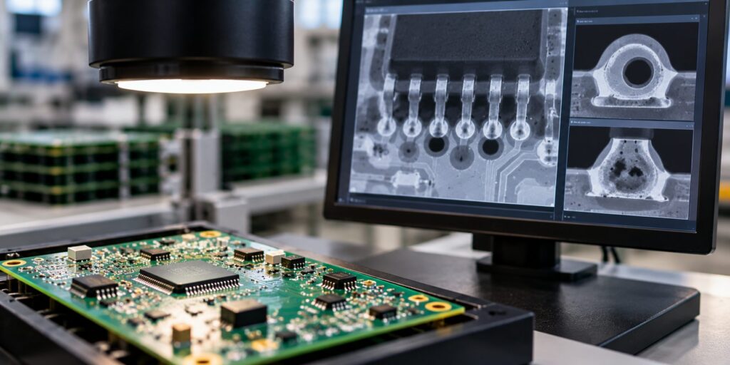
X-ray inspection helps manufacturers identify solder voids and internal defects that may affect thermal performance and long-term reliability.
Solder voids are small pockets of trapped gas or empty space within a solder joint. While some level of voiding can occur naturally during manufacturing, excessive void formation may influence electrical or thermal performance.
This becomes particularly relevant in power electronics and high-current applications. Components generating significant heat rely on effective thermal transfer through solder connections. Excessive voiding can reduce heat dissipation efficiency, potentially increasing operating temperatures. The thermal profile used during assembly can also influence solder joint quality.
X-ray inspection provides visibility into these internal characteristics. Manufacturers can assess void distribution, evaluate solder consistency and determine whether joints meet quality requirements.
Additional defects detectable through X-ray analysis include cold joints, solder bridging and insufficient solder volume. Each presents different risks depending on the application and operating environment.
For example, a power management device with significant voiding beneath its thermal pad may pass initial testing. Over time, elevated temperatures could contribute to accelerated component stress and reduced operational life.
Understanding these risks helps explain why internal inspection remains an important element of reliability-focused manufacturing processes.
Ready to start your project?
Contact our technical team today to see how Altimex can streamline your electronics supply chain.
Contact UsInspection of Complex PCB Assemblies
Complex PCB assemblies often require advanced inspection because increasing component density reduces visibility during standard inspection processes.
Modern electronics continue to evolve towards greater functionality within smaller form factors. This trend introduces additional manufacturing challenges as more components, connections and layers are incorporated into each assembly.
Multilayer PCBs can contain intricate routing structures hidden within the board itself. Dense component placement may limit visibility even when using advanced optical inspection equipment.
Industrial control systems provide a useful example. These products frequently contain compact layouts, mixed-technology assemblies and numerous concealed interconnections. Identifying defects through visual methods alone becomes increasingly difficult.
As assembly complexity increases, manufacturers require greater visibility into hidden features and critical connections. X-ray inspection supports this requirement by enabling examination of areas inaccessible through conventional techniques.
The need for advanced inspection is therefore closely linked to assembly complexity. A straightforward board may require limited internal analysis, while highly integrated electronics can demand significantly greater inspection depth.
Manufacturing confidence depends upon understanding what cannot be seen as much as what can.
Reliability Testing in High-Performance Electronics
High-performance electronics require rigorous inspection and testing processes to maintain long-term operational reliability.
Products operating within demanding environments face conditions capable of exposing weaknesses in assembly quality. Thermal cycling, vibration, electrical loading and environmental stress can place significant demands on solder joints and interconnections.
Inspection forms an important part of reliability assurance because manufacturing defects frequently originate at connection points. Hidden weaknesses may not immediately affect functionality, though repeated operational stress can gradually degrade performance.
Industries such as healthcare, industrial automation and communications infrastructure place particularly high expectations on reliability. Equipment failures can create operational disruption, maintenance costs and reduced system availability.
X-ray inspection supports these environments by helping manufacturers verify assembly integrity before products enter service. Combined with testing and validation processes, it contributes to a more complete understanding of product quality.
Reliability is not achieved through inspection alone. It results from manufacturing discipline, controlled processes, appropriate testing and effective quality assurance throughout production.
Inspection provides visibility. Reliability comes from acting on the information gained through that visibility.
Failure Prevention Through X-Ray Technology
X-ray inspection helps manufacturers identify hidden assembly issues before products reach final testing or deployment.
Early defect detection provides practical advantages throughout manufacturing operations. Issues identified during production can typically be investigated and addressed more efficiently than faults discovered after shipment.
Consider a concealed solder defect beneath a critical component. If detected during inspection, the assembly can undergo corrective action before progressing further through production. If discovered after deployment, the same issue could result in product returns, service costs or operational downtime.
Inspection also supports process validation. Recurring defect patterns may indicate opportunities for manufacturing improvement, allowing engineers to address root causes rather than individual symptoms.
This preventative approach strengthens quality control efforts by reducing the likelihood of hidden defects moving undetected through production.
The objective is not to eliminate risk entirely. Instead, it is to improve visibility, strengthen process control and reduce uncertainty throughout manufacturing workflows.
Compliance With PCB Assembly Standards
PCB inspection processes often support compliance with manufacturing standards and customer quality requirements.
Many industries operate under detailed expectations regarding assembly quality, documentation and traceability. Inspection activities help demonstrate that products have been manufactured according to defined requirements.
IPC standards provide widely recognised guidance for PCB assembly quality and workmanship. While requirements vary between industries and applications, inspection processes frequently support verification activities within broader quality frameworks.
Documentation generated during inspection can contribute to traceability records, manufacturing audits and customer reporting requirements. This becomes particularly important within regulated sectors where evidence of process control may be required.
Medical technology, industrial systems and specialised electronics applications frequently place additional emphasis on quality documentation and manufacturing transparency.
Inspection therefore serves a wider purpose than defect identification alone. It supports accountability, process verification and confidence in manufacturing outcomes.
A structured quality system combines inspection, documentation and traceability to create a clearer picture of overall production performance.
Long Term Product Reliability
Reliable inspection processes support long-term product performance by helping manufacturers identify hidden assembly weaknesses early.
Many electronic products are expected to operate for years within demanding environments. Industrial machinery, infrastructure systems and specialist equipment may experience thousands of operating hours across their service life.
Hidden assembly defects can introduce vulnerabilities that become more significant over time. Thermal expansion, vibration and environmental conditions may gradually place stress on weak solder connections.
By identifying these weaknesses during manufacturing, inspection processes support greater confidence in long-term performance expectations.
Consistency also plays a significant role. Reliable products are not created through isolated inspection activities. They result from repeatable manufacturing processes supported by verification throughout production.
When inspection findings are integrated into quality control workflows, manufacturers gain opportunities to improve process stability and reduce recurring issues.
The result is not a guarantee of future performance. It is a stronger foundation for achieving reliable outcomes across the product lifecycle.
Investment in Advanced PCB Inspection Technology
Investment in advanced inspection technology helps manufacturers improve visibility, consistency and assembly quality within complex PCB production.
As electronic products continue to evolve, inspection requirements evolve alongside them. Smaller components, increased board density and advanced packaging technologies create new challenges for manufacturing teams.
Advanced inspection capability provides manufacturers with greater insight into hidden features, critical interconnections and potential assembly risks. This visibility supports more informed quality decisions throughout production.
The most valuable investment is not the equipment itself. It is the ability to strengthen manufacturing control, improve process understanding and support customer confidence.
For organisations evaluating PCB assembly partners, inspection capability should be considered alongside engineering expertise, process control, testing procedures and quality assurance systems.
A manufacturer’s approach to inspection can provide significant insight into how reliability and consistency are managed across production.
Advanced inspection is ultimately about reducing uncertainty during PCB assembly.
If you are evaluating PCB assembly partners and want to understand how inspection, testing and process control support long-term reliability, Altimex can help. Contact us to discuss suitable manufacturing and quality-control approaches for your product.