

Even small issues in PCB Gerber files can create delays, assembly problems and unnecessary cost once a design reaches manufacturing.
At this stage, many teams assume the design is complete and ready for production handover. In practice, this is where preventable issues often surface. Missing fabrication details, unclear layer data or inconsistent documentation can slow production, trigger repeated clarification requests and introduce risk during assembly.
At Altimex, we regularly work with engineering teams preparing designs for fabrication and assembly. One of the most common causes of avoidable production delays is not a flawed PCB design, but a mismatch between design intent and the manufacturing information provided to production teams.
These problems rarely come from complex engineering faults. More often, they stem from incomplete documentation, missing fabrication requirements or assumptions made during the handover process.
In this guide, we explain what manufacturers need from PCB Gerber files and how engineers can prepare a complete, manufacturing-ready data package. By understanding the production implications behind each file and document, teams can reduce manufacturing friction, improve communication and support a smoother path from design to assembly.
PCB Gerber Files and Their Role in Manufacturing
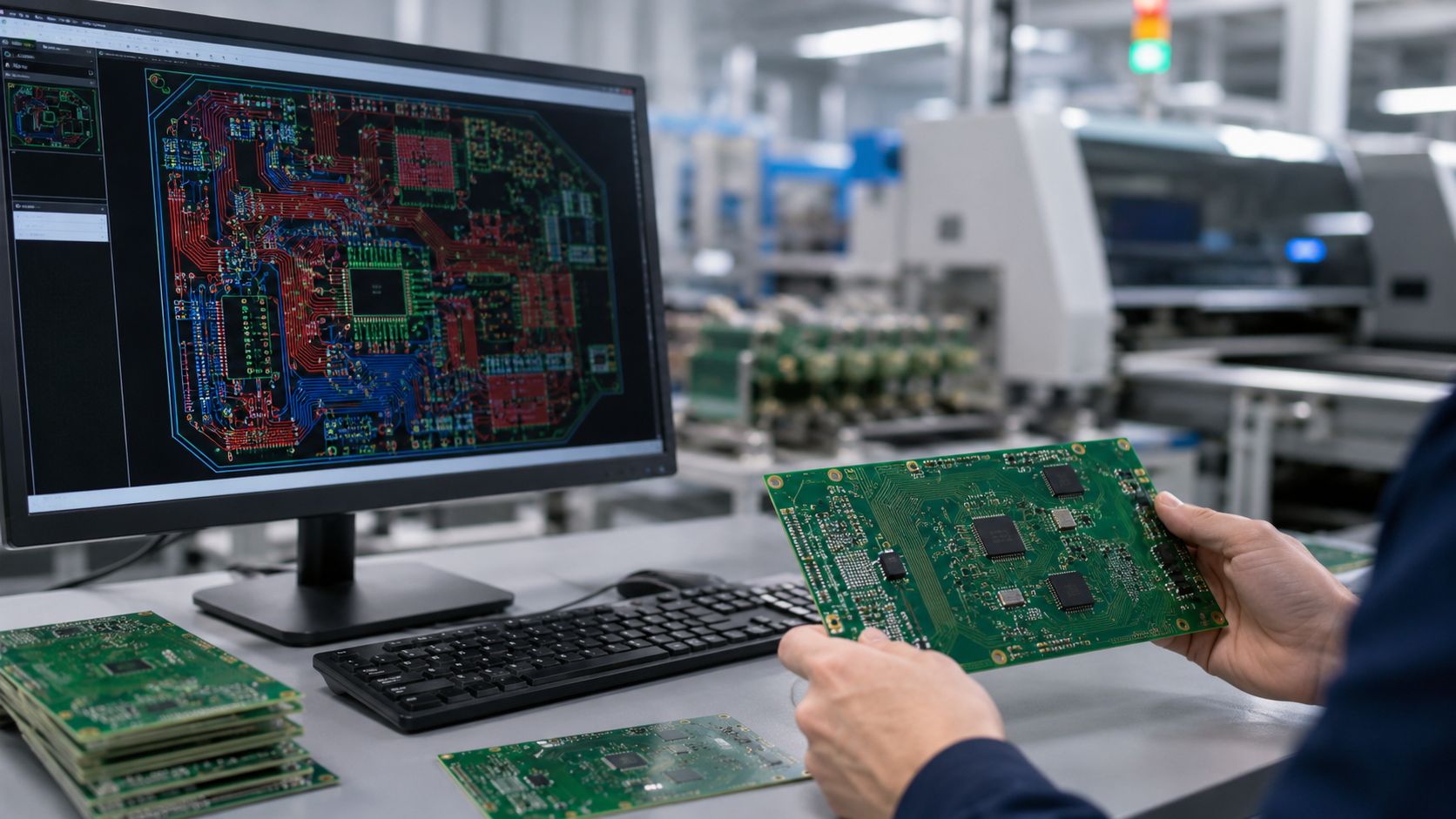
Gerber files provide the manufacturing data required to fabricate PCB layers accurately, making them one of the most important parts of the PCB production process.
They define how each layer should be produced, including:
- Copper traces and pads
- Solder mask openings
- Silkscreen markings
- Board outline geometry
These files are used directly by fabrication equipment to generate imaging, etching and drilling processes. They are not interpreted as design intent. They are treated as manufacturing instructions.
This distinction matters. If data is incomplete, inconsistent or unclear, manufacturers cannot rely on assumptions. Production may pause while clarification is requested or, in some cases, proceed based on interpretations that do not reflect the original design requirements.
At Altimex, we often see delays created by discrepancies between Gerber files and supporting manufacturing documentation. Something as simple as unclear layer naming or inconsistent solder mask definitions can create uncertainty during fabrication and assembly.
A common issue occurs when layer naming does not match the intended structure. Missing polarity definitions, incorrect layer identification or incomplete export settings can create confusion that affects later manufacturing stages.
Gerber files must also align with drill data, stackup information and fabrication notes. If these elements do not match, the risk moves from design into production.
For a broader overview of how manufacturing data flows through production, see our guide to everything to know about the PCB assembly process.
Understanding the role of Gerber files helps engineers treat file preparation as a critical manufacturing activity rather than simply the final export step.
Scale Your Production
From prototype to full-scale electronic assembly, our UK facility is equipped to handle your requirements.
Get a QuoteLayer Alignment and Stackup Accuracy
Incorrect layer alignment or stackup information can create major manufacturing and assembly issues, particularly in multilayer PCB designs.
Stackup documentation defines how the board is physically constructed, including:
- Layer order and function
- Dielectric thickness between layers
- Copper weight
- Controlled impedance requirements
These parameters guide fabrication and help ensure the electrical and mechanical performance of the finished board matches design intent.
Problems arise when stackup information does not align with the submitted manufacturing files. In these situations, manufacturers must request clarification before proceeding, which can introduce avoidable delays.
From a manufacturing perspective, internal layer alignment issues are particularly important in high-speed and high-density designs. Even small inconsistencies can affect impedance performance, signal integrity and long-term reliability.
Accurate stackup documentation helps manufacturers select appropriate processes, materials and tolerances while reducing uncertainty throughout production.
Drill Files and Hole Placement Information
Accurate drill files are essential for ensuring component placement, vias and mounting features align correctly during manufacturing and assembly.
Drill data typically includes:
- NC drill files
- Hole diameters and tolerances
- Plated and non-plated hole definitions
- Via and mounting hole locations
This information must align precisely with copper layers and component footprints. Any discrepancy creates immediate challenges during fabrication or assembly.
One common problem is incorrect hole sizing. If tolerances do not match component specifications, parts may not fit correctly or could place unnecessary stress on solder joints during assembly.
Misaligned drill data can also affect electrical connectivity and mechanical stability. In many cases, these issues only become apparent during assembly or testing, increasing rework and project timelines.
This is one reason why accurate manufacturing data is critical for successful PCB assembly, where component placement accuracy depends on precise alignment between drill information, copper features and component footprints.
At Altimex, drill-related clarification requests are often among the final issues identified before production approval. Ensuring complete and consistent drill data helps minimise delays and supports a smoother manufacturing process.
Engineering-Led Solutions
Work with a team that understands modern electronics and end-to-end manufacturing.
Our ExpertiseBoard Dimensions and Outline Accuracy
Incorrect board dimensions or outline data can prevent PCBs from fitting correctly within assemblies or enclosures.
The board outline defines the physical limits of the PCB and is used by manufacturers to:
- Determine final board shape
- Set edge clearances
- Plan panelisation
- Ensure compatibility with mechanical components
If this data is missing, inconsistent or incorrectly scaled, production cannot proceed with confidence.
A common issue occurs when mechanical drawings and Gerber outline layers do not match. Manufacturers must then determine which version reflects the intended design, creating additional review cycles before fabrication can begin.
In more severe cases, incorrect outline data results in boards that do not fit within enclosures, mounting systems or larger assemblies.
Verifying board dimensions before submission helps ensure the PCB integrates correctly into the final product and reduces avoidable manufacturing delays.
Copper Spacing and Manufacturing Tolerances
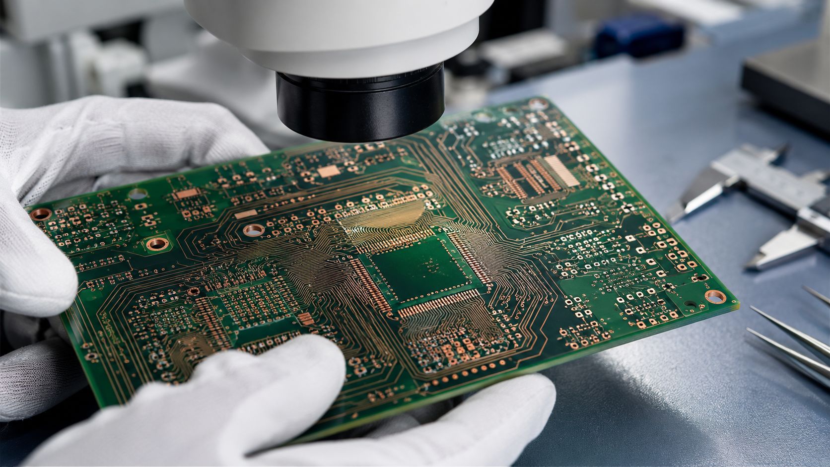
Copper spacing and trace tolerances must align with manufacturing capabilities to avoid production defects and reliability issues.
Fabrication processes operate within defined limits, including:
- Minimum trace width
- Minimum spacing between copper features
- Etching tolerances
- Current carrying capacity
If a design exceeds these limits, manufacturers may not be able to reproduce fine features consistently.
Dense layouts are a common source of manufacturability concerns. A design may pass internal review but still trigger design-for-manufacture feedback once submitted for production. This can result in clarification requests, layout revisions and delays before manufacturing approval is granted.
At Altimex, early manufacturability discussions often help identify tolerance concerns before fabrication begins, reducing the likelihood of production-stage surprises.
Design rules should reflect realistic manufacturing capabilities from the outset rather than relying solely on software validation.
Ready to start your project?
Contact our technical team today to see how Altimex can streamline your electronics supply chain.
Contact UsSilkscreen Placement and Readability
Poor silkscreen placement can create assembly confusion, inspection issues and reduced manufacturing clarity.
Silkscreen information supports production teams by identifying:
- Component reference designators
- Orientation markers
- Assembly identifiers
Common problems include text overlapping pads, designators positioned too close to components and markings that become partially removed during fabrication.
Although silkscreen is sometimes viewed as a secondary design consideration, it plays an important role in assembly efficiency, troubleshooting and inspection.
Clear, readable markings help production teams work more efficiently and support consistent quality control throughout manufacturing.
Material Specifications and PCB Requirements
Manufacturers require clear material specifications to ensure the PCB meets thermal, mechanical and electrical requirements.
Gerber files define geometry, not material performance. Supporting documentation should specify:
- Substrate type and grade
- Copper weight
- Surface finish
- Thermal requirements
- Environmental considerations
Without this information, manufacturers must request clarification or default to standard material selections.
In high-temperature or high-reliability applications, unclear material specifications can create significant performance risks. Selecting the wrong substrate may affect thermal stability, durability and long-term reliability.
Providing complete material information helps ensure the manufacturing process aligns with the operational requirements of the finished product.
Design Rule Checks Before Submission
Running design rule checks before submission helps identify manufacturability problems before they become production delays.
Design Rule Checks (DRC) validation should include:
- Spacing and clearance verification
- Drill size and alignment checks
- Detection of unconnected nets
- Layer consistency reviews
Skipping this step increases the likelihood of issues reaching manufacturing, where they become more disruptive and costly to resolve.
At Altimex, many pre-production queries originate from relatively minor DRC issues that could have been identified during final design review. Resolving these issues before submission helps maintain project momentum and reduces clarification cycles.
Design rule checks should be treated as part of manufacturing preparation, not simply a design-stage exercise.
File Naming and Organisation Standards
Clear file naming and organised documentation reduce confusion and help manufacturers process PCB jobs more efficiently.
A complete manufacturing package should include:
- Clearly named Gerber layers
- Consistent revision identifiers
- Logical folder structures
- Current manufacturing documentation
Poor organisation introduces unnecessary risk.
One common issue involves multiple file revisions being supplied without clear version control. This creates the possibility of outdated data entering production and can result in significant delays if errors are discovered after fabrication has started.
Consistent naming conventions and structured documentation help ensure manufacturers are working from the correct information throughout the production process.
Fabrication Notes and Manufacturing Instructions
Fabrication notes help manufacturers understand design intent, special requirements and production constraints that may not appear directly in Gerber files.
Important fabrication notes often include:
- Tolerance requirements
- Controlled impedance specifications
- Surface finish requirements
- Special processing instructions
- Testing requirements
Without this information, manufacturers must rely on assumptions or standard defaults.
A common example is controlled impedance. If impedance requirements are not documented clearly, a PCB may be fabricated successfully according to the Gerber data while still failing to meet performance expectations in operation.
Detailed fabrication notes improve communication, reduce clarification requests and help ensure the finished PCB reflects the original engineering intent.
Communication With PCB Manufacturers
Clear communication between engineers and PCB manufacturers helps reduce delays, avoid assumptions and improve production outcomes.
Many manufacturing issues arise from communication gaps rather than design errors. Early collaboration helps identify concerns before they affect production schedules.
Effective communication should include:
- Early design-for-manufacture discussions
- Clear revision control
- Defined approval stages
- Accessible technical contacts
At Altimex, we often find that the most successful projects involve collaboration before fabrication begins rather than problem-solving after issues have been identified.
Early feedback can highlight manufacturability concerns, material considerations and assembly requirements while changes are still straightforward to implement.
Treating your manufacturing partner as part of the engineering process helps reduce production risk and supports more predictable outcomes.
Preparing PCB Gerber Files for Manufacturing Success
Accurate Gerber files are only one part of a successful PCB manufacturing package. Supporting documentation, clear communication and manufacturability checks all contribute to a smoother production process.
By reviewing stackups, drill data, fabrication notes and design rule compliance before submission, engineers can reduce avoidable delays and help ensure designs move efficiently into fabrication and assembly.
If you are preparing PCB files for production and want to reduce manufacturing delays or assembly issues, Altimex can help review manufacturing requirements before fabrication begins. Contact us to discuss your project and ensure your manufacturing data is ready for production.